
Контрактное производство электроники под ключ в Китае
Шэньчжэнь, район Баоань, улица Фуюн, улица Фуцяо, район 3, промышленный парк Лонгхуй 6


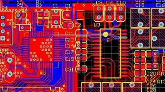
With the rapid development of modern electronic technology, PCBA also develops towards high density and high reliability. Although the level of PCB and PCBA manufacturing technology has been greatly improved, conventional PCB solder resistance process will not have a fatal impact on product manufacturability. However, for the devices with very small pin spacing, the unreasonable design of PCB welding pad and PCB welding pad will increase the difficulty of SMT welding process and increase the quality risk of PCBA surface mounting processing.
In view of the hidden problems of manufacturability and reliability caused by the unreasonable design of PCB welding aid and solder pad, the manufacturability problems can be avoided through the optimization design of device packaging combined with the actual technological level of PCB and PCBA. Optimization design mainly from two aspects, first, PCB LAYOUT optimization design; Second, PCB engineering optimization design.
Current status of PCB solder resistance design
PCB LAYOUT design
According to IPC 7351 standard package library and refer to the device specification recommended pad size package design. In order to fast design, Layout engineers give priority to enlarging and modifying the design according to the recommended size of the welding pad. The length and width of the PCB welding aid pad are increased by 0.1mm, and the length and width of the welding resist pad are also increased by 0.1mm on the basis of the welding aid pad. As shown in Figure 1:
PCB engineering design
Conventional PCB solder resistance process requires that the edge edge of the aid pad be covered by 0.05mm, and the middle solder bridge of the two aid pads be larger than 0.1mm, as shown in Figure 2 (2). In the stage of PCB engineering design, when the size of the solder pad cannot be optimized and the solder bridge between the two pads is less than 0.1mm, PCB engineering adopts the group welding plate window design. As shown in Figure 2 (3) :

PCB LAYOUT design requirements
When the edge distance between two auxiliary pads is greater than 0.2mm, the packaging is designed according to the conventional pads; When the edge distance between two aid pads is less than 0.2mm, DFM optimization design is needed. The DFM optimization design method is helpful for the size optimization of welding pads and welding resistance pads. Ensure that the solder resistance from the solder resistance process forms the minimum solder bridge isolation pad during PCB manufacturing. As shown in Figure 3:
PCB engineering design requirements
When the spacing between the edges of the two auxiliary welding pads is greater than 0.2mm, engineering design shall be carried out according to the conventional requirements; When the edge distance between two pads is less than 0.2mm, DFM design needs to be carried out. The engineering DFM design methods include welding resistance layer design optimization and welding assistant layer cupping treatment. The size of the copper cutting must refer to the device specifications. The solder pad of the auxiliary layer after the copper cutting should be within the size range of the recommended design of the solder pad, and the PCB solder resistance design should be single-plate window design, that is, the solder bridge can be covered between the solder pads. Ensure that during the manufacturing process of PCBA, the two pads are separated by solder resistance bridge to avoid welding appearance quality problems and electrical performance reliability problems.
PCBA process capability requirements
Welding resistance film can effectively prevent solder bridge short bonding in the process of welding and assembly. For PCB with high density and fine spacing pins, if the open weld bridge between pins is isolated, PCBA processing plant cannot guarantee the local welding quality of products. For PCB isolated by high density and fine spacing pin open weld, the current processing method of PCBA manufacturing factory is to determine the quality of PCB incoming materials, and do not go into production. If the customer insists on going online, the PCBA manufacturing plant will not guarantee the welding quality of the product in order to avoid quality risks. The welding quality problems in the manufacturing process of the PCBA factory will be negotiated and dealt with.
Case study
Device specification dimensions
As shown in Figure 4 below, center spacing of device pins is 0.65mm, width of pins is 0.2 ~ 0.4mm, length of pins is 0.3 ~ 0.5mm.
PCB LAYOUT Actual design
As shown in Figure 5 below, the size of the auxiliary pad is 0.8 * 0.5mm, the size of the resist pad is 0.9 * 0.6mm, the center spacing of the device pad is 0.65mm, the spacing of the auxiliary edge is 0.15mm, the spacing of the resist edge is 0.05mm, and the width of the unilateral resist welding is increased by 0.05mm.
Summary of optimal design
To sum up, the chip with the edge spacing of the device pins less than 0.2mm cannot be designed in accordance with the conventional package, and the width of the auxiliary pad is not compensated in the design of PCB LAYOUT. The reliability of the welding contact area can be avoided by lengthening the length of the auxiliary pad. If the gap between the two welding resistance edges is too small due to the large welding pad, priority should be given to cupping. If the design of the solder shield is too large, the solder shield design should be optimized to effectively increase the width of the edge of the two solder shield pads, so as to ensure the welding quality of PCBA. It can be seen that the coordination between welding aid and welding resistance pad design plays a decisive role in improving PCBA manufacturability and welding pass-through rate.


Достаточно загрузить файлы Gerber, BOM и проектные документы, и команда KINGFORD предоставит полное предложение в течение 24 часов.