
Контрактное производство электроники под ключ в Китае
Шэньчжэнь, район Баоань, улица Фуюн, улица Фуцяо, район 3, промышленный парк Лонгхуй 6

The test coupon is used to measure whether the characteristic impedance of PCB boards meets design requirements by using Time Domain Reflectometer (TDR). Generally the impedance to be controlled has two cases of single wire and differential pairs. Therefore, the line width and line distance (if there is a difference match) on the test coupon must be the same as the lines to be controlled.
The most important thing to measure is the location of the ground point. In order to reduce the inductance value of the ground lead, the ground point of the TDR probe is usually very close to the probe tip of the measurement signal. Therefore, the distance between the point of the measurement signal and the ground point on the test coupon and the method should be consistent with the probe rod used.
1. In high-speed PCB design, copper can be applied to the blank area of signal layer, and how to distribute the copper applied to multiple signal layers in grounding and power supply?
Generally in the blank area of copper application most of the situation is grounded. Just pay attention to the distance between the copper and the signal line when applying copper beside the high-speed signal line, because the copper will reduce the characteristic impedance of the line a little. Also be careful not to affect the characteristic impedance of its layer, for example, in the dual strip line structure.
2. Can the signal line above the power plane use the microstrip line model to calculate the characteristic impedance? Can the signal between the power supply and the ground plane be calculated using the banded line model?
Yes, both the power plane and the ground plane must be considered as reference planes when calculating the characteristic impedance. For example, four-layer board: top layer - power layer - ground layer - bottom layer. In this case, the characteristic impedance model of the top layer is a microstrip line model with the power plane as the reference plane.
3. Can the software automatically generate test points on high density printed boards meet the test requirements of mass production in general?
Whether the automatic generation of test points in general software can meet the test requirements depends on whether the specification of adding test points meets the requirements of test machines. In addition, if the wiring is too dense and the specification for adding test points is strict, it may not be possible to automatically add test points to each segment of the line. Of course, it is necessary to manually complete the test place.
4. Will adding test points affect the quality of high-speed signals?
Whether this affects the quality of the signal depends on how the test point is added and how fast the signal is. Basically, additional test points (without an existing in-line punch (via or DIP pin) as test points) may be added to the in-line or a short line pulled out of the in-line. The former is equivalent to adding a small capacitor to the line, the latter is an extra branch. Both of these conditions will affect the high-speed signal more or less, and the extent of the impact is related to the frequency speed and edge rate of the signal. The size of the effect can be determined by simulation. In principle, the smaller the test point, the better (of course, to meet the requirements of the test machine), the shorter the branch, the better.

5, a number of PCB system, how to connect the ground wire between the boards?
When the signal or power supply between each PCB board is operated, for example, when the power supply or signal is sent to board B, there must be an equal amount of current flowing back to board A from the ground layer (this is Kirchoff current law). The current in this formation will flow back where it has the least resistance. Therefore, the number of pins assigned to the formation should not be too small to reduce impedance at the junctions where both power and signal are connected to each other, thus reducing noise in the formation. Alternatively, it is possible to analyze the entire current loop, especially the part where the current is high, and adjust the ground or ground connection to control the path of the current (for example, by creating a low impedance in one place so that most of the current passes through it), reducing the impact on other, more sensitive signals.
6. Can you introduce some foreign technical books and data on high-speed PCB design?
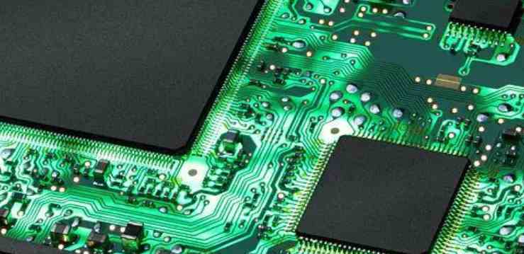
High - speed digital circuits are now used in related fields such as communication networks and computers. In the communication network, PCB board working frequency has reached around GHz, the number of layers as far as I know up to 40 layers. Computer related applications also because of the progress of chips, no matter the general PC or Server (Server), the highest working frequency on the board has reached 400MHz (such as Rambus) or more. blind/buried vias, mircrovias, and build-up processes are increasingly in demand in response to high speed and high density wiring. All of these design requirements are mass-produced by manufacturers.
7. Two commonly referred characteristic impedance formulas:
microstrip Z={87/[sqrt(Er+1.41)]}ln[5.98H/(0.8W+T)], where, W is the wire width, T is the thickness of the copper wire, H is the distance from the wire to the reference plane, Er is the dielectric constant of the PCB sheet. This formula must be in 0.1< (W/H)< 2.0 and 1< (Er)< 15 can only be applied.
stripline Z=[60/sqrt(Er)]ln{4H/[0.67π(T+0.8W)]}, where H is the distance between the two reference planes, and the line is located in the middle of the two reference planes. This formula must be in the W/H< 0.35 and T/H< 0.25 can only be applied.

Line impedance
2023-03-30


Достаточно загрузить файлы Gerber, BOM и проектные документы, и команда KINGFORD предоставит полное предложение в течение 24 часов.