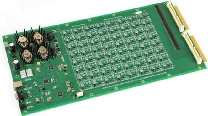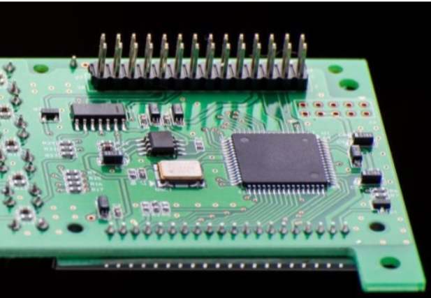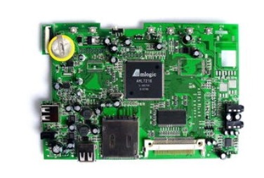
MCP (Multiple Chip Package) memory, MCP is in a plastic package shell, vertical stacking of different sizes of various types of memory or non-memory chips, is a one level single package hybrid technology, using this method to save the space of small printed circuit board PCB.
3D wafer level packaging, English abbreviation (WLP), including CIS transmitter, MEMS package, standard device package. It refers to the packaging technology of stacking more than two chips vertically in the same package without changing the package size. It originates from the stacking packaging of flash memory (NOR/NAND) and SDRAM. The main features include: multi-function, high efficiency; Large capacity, high density, double function and application per unit volume and low cost.
One: the packaging trend is laminated seal (PoP); Low-yield chips seem to favor PoP.
Two: multi-chip package (MCP) method, and high density and high performance chips tend to MCP.
Three: System level packaging (SiP) technology is the main technology, where logic and memory devices are manufactured in their own processes and then combined in a SiP package.
Most flash memory today uses a Multichip Package (MCP), which usually packages ROM and RAM together. Multi-core packaging (MCP) technology is to assemble various micro components (bare chips and chip components) that constitute electronic circuits on high-density multi-layer interconnected substrates, and form high-density, high-performance and highly reliable micro-electronic products (including components, components, subsystems and systems). Technically, MCP pursues high speed, high performance, high reliability and multi-function, unlike the conventional hybrid IC technology which focuses on reducing volume and weight. However, as Flash flash and DRAM flash pursue the minimization of volume, this packaging technology has disadvantages in bandwidth and space proportion due to the use of wire welding, and WSP packaging technology will be a better solution.

2. Factors affecting the assembly quality of BGA patches
Feasibility of BGA pad design
BGA packages are classified into several types according to different tones. In general, the feasibility of CAD tracing and the manufacturability of PCB (printed circuit board) should be considered first in BGA pad design. BGA pads also come in a variety of types, and the following commonly used types can be freely chosen within the space allowed.
Dog bone pads use holes to direct the trace to other layers, so there are some limitations on the size of the pads. Due to the presence of holes, some defects are often caused in the PCB manufacturing process, such as welding bridge due to the loss of the solder resistance layer. Therefore, the size of the pad must be designed strictly in accordance with the actual manufacturing level to minimize the welding defects in the BGA welding process and leave some room for future BGA rework.
• Through holes are externally allocated to BGA pads
This type of pad is best suited for BGA components with low I/O volume. This type of pad design provides convenience for welding and allows more freedom for pad size. Of course, basic requirements must be met when it comes to tracking. Therefore, it is almost impossible to utilize this pad on BGA with higher I/O numbers.
With the development of microporous technology in PCB manufacturing, the perforation of solder pad develops.
In addition to pad type, the position of the choke layer and BGA pad is directly related to BGA welding. BGA pads are classified into two types according to different choke layer positions: SMD (defined as choke layer) pads and NSMD (undefined choke layer) pads, which respectively play a role in BGA welding. When SMD pad is used, the bonding area between pad and pad is large, resulting in the bonding area between solder joint and PCB board is quite large. However, as the size of the pad increases, the spacing between adjacent pads decreases, which affects the distribution and tracking ability of the pad.
BGA pads are not affected if the solder resistance film deviates in the same direction during PCB manufacturing, which is advantageous for BGA welding. However, this type of pad tends to break when the edge is reworked by the solder resistance layer, which is not conducive to the rework effect. Once the NSMD pad is used, the pad will be relatively small, which facilitates the distribution and tracking of the through-hole pad. However, this type of pad structure results in a reduction in the bonding area between the solder joint and the pad, and further decreases the bonding strength of the solder joint. In short, both pads have their own advantages and disadvantages, and the corresponding pads can be determined based on technical considerations.
Solder paste printing
Solder paste printing plays a key role in determining welding quality. Solder paste printing is the accurate conversion of solder paste from template to pad, which includes solder paste, solder paste and press. The accuracy of the paste press shall first conform to the requirements of BGA assembly. The template determines the amount of solder paste by its thickness and opening size. The amount of solder paste required for BGA packaging is usually determined by three aspects:
• Sufficient solder should be used to ensure good BGA welding.
• The amount of solder paste should compensate for the ball coplane error (usually 0.1mm) of the BGA component.
• When there are other fine-spaced components on the board, the amount of solder paste should be taken into account to prevent more welding defects.
Positioning accuracy
The exact location of the BGA component on the circuit board is entirely dependent on the accuracy of the chip mounter, most of which include a specific positioning system that helps to achieve accurate positioning of the BGA component. In addition, some chip paste machines can even check the coplanicity of BGA welding balls and identify some defects, such as missed balls, which is very helpful to improve the reliability of BGA welding.
In addition, a number of other measures can be taken to further improve the installation accuracy of BGA components. For example, local reference marks are set on the outside of the BGA pad, or several fold lines are set to manually inspected reference marks after assembly, both of which have been proven in actual manufacturing.
In addition, because of the surface tension of the solder, the BGA component has an obvious self-centering effect in the welding process, so some designers in the design of BGA pad deliberately add pads on the four corners, so that the self-centering effect is more obvious, to ensure that the BGA component can shift the installation position after automatic reset.
Welding temperature curves and welding defects
Welding temperature curve directly determines welding quality. The temperature curve usually consists of four stages: preheating, soaking, reflux, and cooling, each with a different physical/chemical change. As the setting of temperature curve determines the formation process of solder joint, it is closely related to the reliability of solder joint. Because of the particularity of BGA packaging, it is very difficult to generate a satisfactory temperature curve. In general, BGA components need to measure three temperatures: package temperature, board surface temperature, and BGA internal solder joint temperature.
BGA inspection and rework techniques
Because all BGA solder joints are under the packaging after welding, traditional inspection methods (such as fly pin testing or visual inspection) cannot meet the actual requirements. To date, the leading methods that can scan for defects in BGA solder joints are AOI (Automatic Optical inspection) testing and AXI (Automatic X-ray inspection) testing.
Due to the characteristics of BGA construction, it is almost impossible to inspect individual solder joints of BGA components. However, the entire package should be repackaged.
Other factors
Other factors must be taken care of during BGA assembly, such as electrostatic protection and baking of BGA components. Typically, BGA components require special packaging with electrostatic protection requirements. When assembling a printed circuit board, take strict ESD measures, including grounding the device, personnel management, and environment management.


