
Контрактное производство электроники под ключ в Китае
Шэньчжэнь, район Баоань, улица Фуюн, улица Фуцяо, район 3, промышленный парк Лонгхуй 6

According to product standards, the term "clean free" means that the residues of PCB circuit boards are safe from a chemical point of view, will not have any impact on the PCB circuit board production line, and can be left on the PCB board. Corrosion, SIR, electromigration, and other specialized tests are used to determine the halogen/halide content to ensure the safety of the clean-free assembly after completion.
However, even if the use of low solid content of the free cleaning flux, there will still be a lot of residues, for high reliability requirements of the product, in the PCB circuit board is not allowed to allow any residues and pollutants. For military applications, even washless electronic assemblies are required to be cleaned.
Resin residue that is not removed before surface coating may cause lamination or cracks in the protective layer; The surfactant residue may cause electrochemical migration under the coating, resulting in the failure of the coating rupture protection. Studies have shown that by cleaning can increase coating bond rate by 50%.
The most intuitive impact of PCBA pollutants is the appearance of PCBA. If it is placed or used in a high temperature and humidity environment for a long time, the residue may absorb moisture and become white. Due to the large number of leadless chips, micro-BGA, chip-level package (CSP) and 01005 used in the components, the distance between components and PCB board is reduced, the size is minisized, and the assembly density is increasing. If the halide is hidden under the element where it cannot be cleaned, local cleaning may result in irreversible consequences due to the release of the halide.
Cleaning technology is the future development direction, must set up pure water source and discharge water treatment workshop. It uses water as cleaning medium, and adds surfactants, auxiliaries, corrosion inhibitors, chelating agents and so on to form a series of water-based cleaning agents. Can remove water solvent (flux is water soluble) and non-polar pollutants.
Therefore, in order not to affect the service life of the pcba board, cleaning steps are necessary.

2. Summary of experience in PCB board proofing and drawing
PCBA patch factory: Summary of experience in PCB board proofing and drawing
(1) : When drawing the schematic diagram, the pin must be marked with network NET rather than TEXT, otherwise there will be problems when guiding PCB design
(2) : When drawing the schematic diagram, all components must be packaged, otherwise the components will not be found when guiding PCB
Some components can not be found in the library is to draw their own, in fact, or their own drawing, and finally have a library of their own, that is convenient. To do this, launch FILE/NEW-- select SCH LIB-- and enter the Parts editing library -- and then click TOOLS-RENAME on the COMPONENT to rename the component.
The drawing of component encapsulation is the same as this one, but PCB LIB is selected, and the frame of component is in TOPOverlay layer, which is yellow.
(3) : Rename the symbols in order after drawing, select TOOLS ---- and ANNOTATE and select the order
(4) : Before conversion into PCB, to generate reports, mainly network table selection DESIGN ---- Creat Netlist create network table
(5) : There is also to check the electrical rules: choose TOOLS --. > ERC
(6) : Then PCB can be generated. If there is any error in the generation process, the schematic diagram must be modified correctly to regenerate PCB
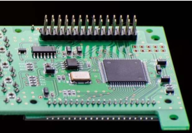
(7) : PCB must first step a good board, should let the line go as short as possible, as few holes as possible.
(8) : Design rules before drawing lines: TOOLS -- Design Rules. The Clearance Constrain GAP in Routing can be configured as 10 or 12. Set the aperture in ROUTING VIA STYLE, the maximum outer diameter, the minimum outer diameter, the maximum inner diameter, and the minimum inner diameter of the Han disk. The WIDTh Constraint sets the width of the line, maximum and minimum
(9) : The width of the drawing line is generally 12MIL, the peripheral circle of power and ground is 120 or 100, the power and ground of the film is 50 or 40 or 30, the crystal town line should be thick, to be placed next to the MCU, the common line should be thick, the long line should be thick, the line can not turn the right Angle to 45 degrees, the power and ground and other signs must be marked in TOPLAY, Convenient debugging wire.
If you find the diagram is not correct, you must first change the schematic diagram, and then use the schematic diagram to change the PCB.
10) : The option at the bottom of the VIEW option can be inch or mm.
(11) : In order to improve the anti-interference of the PCB board, it is best to apply copper at last. Select the icon of applying copper, and a dialog box appears. In the figure, Net Option selects the connected network, and the two options below it should be selected, HATCHING STYLE, and select the form of applying copper. The GRID SIZE is the copper grid spot spacing, the TRACK WIDTH should be consistent with the line width we have drawn PCB, and the other two items can be treated by using the LOCKPrimitives
MCP POP with SIP package
2023-02-22


Достаточно загрузить файлы Gerber, BOM и проектные документы, и команда KINGFORD предоставит полное предложение в течение 24 часов.