
Контрактное производство электроники под ключ в Китае
Шэньчжэнь, район Баоань, улица Фуюн, улица Фуцяо, район 3, промышленный парк Лонгхуй 6

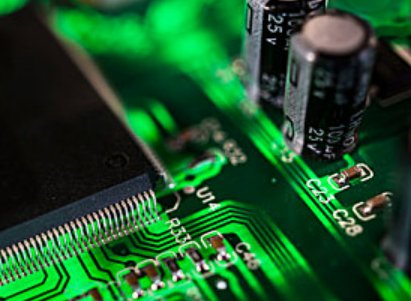
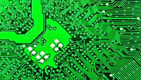
The green or brown on the PCB is the color of solder mask. This layer is an insulating protective layer that protects the copper wire and prevents parts from being welded in incorrect places. A silk screen will be printed on top of the solder resistance layer. It is usually printed with words and symbols (mostly white) to indicate the position of the parts on the board. Screen printing is also known as legend.
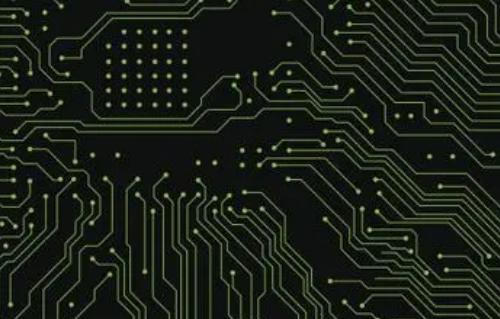
The printed circuit board etches the complex circuit copper wire between parts on a board after meticulous and neat planning. It provides the main support body for the installation and interconnection of electronic components, and is an indispensable basic part of all electronic products.
Printed circuit board A flat plate made of non-conductive material, usually with pre-drilled holes designed to hold chips and other electronic components. The holes of the components help to connect the pre-defined metal paths printed on the surface of the board electronically. After the connectors of the electronic components are passed through the PCB, a conductive metal electrode is attached to the PCB to form a circuit.
4. Brief history and development direction of PCB
A brief history of development: China began the development of single-sided printed board from the mid-1950s, first used in semiconductor radio. In 1960 s, we developed our coated foil substrate by ourselves and made copper foil etching become the dominant technology of PCB production. In 1960 s, we could produce single panel in large quantity. Small batch production of double-sided metallized hole printing, and in a few units began to develop multilayer plates. In 1970s, graphic electroplating etching process was popularized in China, but due to various interference, special materials and special equipment for printed circuits did not catch up in time, and the whole production technology level fell behind the advanced level of foreign countries. In the eighties due to the approval of the reform and open policy, it not only introduced a large number of single, double-sided and multi-layer printed board production lines which have the advanced level of foreign in the eighties, but also improved the production technology level of printed circuits in our country after more than 10 years of digestion and absorption.

Development direction: In recent years, China's electronics industry has become one of the main pillars driving domestic economic growth. With the rapid development of computer, communication equipment, consumer electronics and automobile industries, PCB industry has also achieved rapid development. With the development of printed circuit products, new materials, new technology and new equipment are required. Printed electrical equipment material industry in our country should pay more attention to improving performance and quality while expanding output. Printed circuit special equipment industry is no longer low-level imitation, but to the production of automation, precision, multifunctional, modern equipment development. PCB production set the world's high technology in one, printed circuit production technology will use liquid photographic imaging, direct plating, pulse plating, laminated multilayer board and other new processes.
Five, PCB characteristics and classification as well as upstream and downstream
PCB features high density, high reliability, designability, producibility, assembly and maintainability of six aspects.
Generally speaking, the more complex the function of electronic products, the longer the loop distance, the more contact pin number, the more PCB layer required, such as high level consumer electronics, information and communication products; The soft board is mainly used in products that need to be wound: such as notebook computers, cameras, automobile instruments, etc. PCB classification according to the number of layers, can be divided into single panel (SSB), double panel (DSB) and multi-layer board (MLB); According to the softness, it can be divided into rigid printed circuit board (RPC) and flexible printed circuit board (FPC). In industrial research, according to the above basic classification of PCB products, the PCB industry is generally subdivided into six major sub-industries, such as single panel, double panel, conventional multilayer board, flexible board, HDI(high density sintering) board and packaging substrate.
Upstream PCB industries include PCB substrate board raw material suppliers and PCB production equipment suppliers, while downstream industries include consumer electronics, computer and peripheral products, automotive and mobile phone industries. According to the industry chain, it can be divided into raw materials - copper clad plate - printed circuit board - electronic products application. Specific analysis is as follows:
Glass fiber cloth: Glass fiber cloth is one of the raw materials of copper clad plate, made of glass fiber yarn textile, accounting for about 40% of the cost of copper clad plate (thick plate) and 25%(sheet). Glass fiber yarn is calcined into liquid by silica sand and other raw materials in the kiln. It is drawn into very fine glass fiber through a very fine alloy nozzle. Then hundreds of glass fiber are twisted into glass fiber yarn.
Copper foil: Copper foil is the largest proportion of copper clad plate cost raw materials, accounting for about 30% of the cost of copper clad plate (thick plate) and 50%(sheet), so the price rise of copper foil is the main driving force for the price rise of copper clad plate.
Copper clad plate: Copper clad plate is the product of glass fiber cloth and copper foil pressed together by epoxy resin and other fusion agents, which is the direct raw material of PCB. It is made into printed circuit board after etching, electroplating and multilayer plate pressing.


Достаточно загрузить файлы Gerber, BOM и проектные документы, и команда KINGFORD предоставит полное предложение в течение 24 часов.