
Контрактное производство электроники под ключ в Китае
Шэньчжэнь, район Баоань, улица Фуюн, улица Фуцяо, район 3, промышленный парк Лонгхуй 6

What problems should we pay attention to in PCB laminated design? Let a professional engineer tell you. Two rules must be followed in the design of lamination:
Each routing layer must have an adjacent reference layer (power supply or stratum);
2. The adjacent main power layer and the ground should be kept at a minimum distance to provide a large coupling capacitance.
The electromagnetic compatibility of single-layer board and double-layer board is becoming more and more prominent. The main reason for this phenomenon is that the signal loop area is too large, which not only produces strong electromagnetic radiation, but also makes the circuit sensitive to external interference. The simplest way to improve the electromagnetic compatibility of a circuit is to reduce the loop area of key signals.
The key signal mainly refers to the signal that produces strong radiation and the signal that is sensitive to the outside world. Single and double layer plates are usually used in low frequency simulation designs below 10 KHZ: 1) the power supply in the same layer is routed in a radial manner and the sum of the length of the lines is minimized; 2) When walking the power supply and ground wire, close to each other; Lay a ground wire near the key signal wire as close as possible. Thus, a smaller loop area is formed and the sensitivity of differential mode radiation to external interference is reduced. 3) If it is a double-layer circuit board, it can be on the other side of the circuit board, close to the signal line below, along the signal line, the line as wide as possible. 2 Stacking four Layers 1. Sig-gnd (PWR)-PWR (GND)-SIG; 2. GND-SIG(PWR)-SIG(PWR)-GND; The above two laminated design, the potential problem is for the traditional 1.6mm (62mil) plate thickness. The layer spacing will become very large, which is not conducive to control impedance, interlayer coupling and shielding. In particular, the large spacing between the power supply strata reduces the plate capacitance and is not conducive to noise filtering.
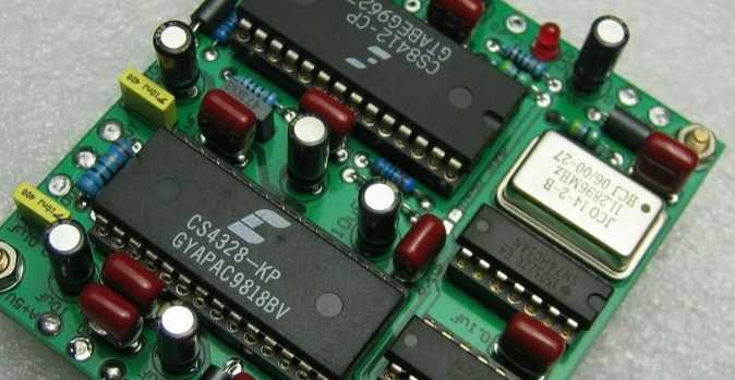
This document mainly introduces the schematic diagram of H6 chip and the key points and precautions of PCB design to ensure the quality of hardware design.
1) SOC has two sets of crystal oscillators, and both sets of crystal oscillator circuits are retained in the design. The default figure 2 is DCX0 crystal oscillator circuit patch, and the device NC of 24M crystal oscillator circuit 1.
2) RTC low-frequency crystal oscillator circuit through the internal RC calibration circuit, can fanout 5ppm 32K, DCX0 crystal oscillator circuit can fanout24Mclock signal. If DCXO is turned off in a standby scenario, the timing switch of DCX0 will be adjusted internally. In this case, the accuracy of 32K signal will be affected, resulting in a timing accuracy error of 4s/ hour. If the timer accuracy is required, the 32K clock circuit should be retained.
3) The accuracy of external 24M crystal oscillator is required to be less than +/-10ppm, and can work stably at high temperature of 70°C and low temperature of -20°C;
4) In order to ensure WIFI performance, it is recommended to use the whole-verified crystal oscillator model 160606E3SB24E004304E.
5) The external matching capacitor is 18pF, and the matching capacitance is selected according to the load capacitance of the crystal;
6) The R1 serial resistor needs to reserve a position for the convenience of debugging the amplitude of oscillation;
Precautions for emi emc PCB layout

Consider EMI layout
First, line
Ii. VCC&GND cutting
Three, EMI related components placement
Four, grounding
Five, the problem of multilayer board
First, line
1. Routing (high-speed line processing)
A. High-speed line (CLK,...) Avoid cross-cutting, avoid walking near the edge of the board (50 mils) and the cutting line, avoid walking under the Slot and the dense area of the Via, try to change layers as little as possible (priority from high to low), and ensure the integrity of the high-speed line reference surface.
B and CLK are the best way to wind the same length. The distance between parallel lines is large (at least more than 3 times the line width) and the coupling length is as small as possible. (Figure below) and irregular winding or spiral winding is better than regular snake winding. Try to avoid winding near IC, Slot, I\O, preferably when the reference plane is complete.
2. Routing (differential line processing)
A. The return current of differential routing will also walk on the reference plane, and most of it will be on the reference plane. Also try to avoid cross-cutting problems, as shown in the figure below:
B. The matching of differential routing is more important than the matching of line length, which has a greater impact than the unequal spacing.
a. Single-channel signal electromagnetic field distribution b. Differential routing electromagnetic field distribution
3. Routing (isolation)
A, CLK, IO (30 mils), Power trace&shape (20 mils) and other signal cables (30 mils) that need external cable have spacing requirements.
B. Irrelevant routing (Power trace in most cases) should be kept away from the CLK region and I/O region to avoid interference by the CLK region and interference with the I/O region.
C, AGND and GND area go line to distinguish strictly, to avoid each other the phenomenon.
D. The companion ground wire is optional for EMI. It should be ensured that there is enough spacing between it and other signal wires to meet EMI requirements (20-30 mils). But considering the signal quality to have a companion ground wire, it is necessary to hit enough underground Via, spacing within 800 mils.
Ii. VCC&GND cutting
1. Cutting (I\O)
VCC and GND cutting lines at A and Back I\O should be consistent as far as possible. The cutting lines mainly refer to parts placement and routing. Generally, under the transformer below the Bead, the GND pin of the bypass capacitor is required to be in the I\O area. Avoid crossing between two sides of the cable. There is no cutting line between each I\O in the I\O zone. Influence: crossing of lines > Not consistent.
B. Is it cut in Front of USB, 1394, COM, GAME and Panel? According to the actual situation, if cutting will cause a lot of cross-cutting, or make the VCC and GND layer become very fragmentary, do not cut. Advantages: Can ensure the integrity of VCC, GND, has low impedance.
2. Cutting (CLK)
A. In general, the VCC layer is cut into CLK-VCC and the GND layer is cut with a notch, or the VCC layer is cut into GND and the GND layer is not cut. Depending on the actual situation, VCC and GND can not be cut. If many CLKS can be passed through the Top layer in one go without changing layers, the VCC layer is also not cut. Advantages: Ensure the integrity of VCC and GND, reduce CLK multiple layer changes.
3. Cutting (Audio area)
A, AGND and GND area also refer to parts of parting line, required parts to distinguish, when putting in their respective regions, at the same time there is AGND &gnd component parts put on the cutting line, easy to cut. (Similar for I\O zone)
B, VCC and GND are also well cut and consistent with each other to avoid cable crossing, and the effects are as follows: cable crossing > Inconsistent cutting.
Three, EMI related components placement
1. High-speed IC and decoupling capacitor
A, high-speed IC avoid side or near I\O area.
B. Decoupling capacitor is mostly located near large high-speed IC, such as North-South bridge... , main functions: charge and discharge voltage regulation and filtering. So try to close to the power supply pin.
C. Another kind of capacitor, namely capacitor often reserved by EMI, is mainly located near the CLK layup (to ensure the integrity of CLK return current), near high-speed IC (filtering to prevent IC noise from affecting the surrounding area) or near I\O power source (reducing the influence of this power source on I\O).
2. bypass capacitor
A. The Bypass capacitor must be placed at the nearest I\O At the Connector, the correct connection method is as follows: directly through the capacitor Pin to the Connector, without any branch (to reduce the inductance effect of the high frequency wire). The capacitor in CLK's RC circuit has the same connection requirement (RC should be placed at the CLK source).
Four, grounding
Do not lay GND shapes at random on the A, Top, and Bottom cabling layers. If there is one, there should be enough GND Via (poor grounding may cause antenna effect).
B and I\O areas should have enough GND Via through each layer, and the fixed pin of the connector should also be connected to GND through Via.
pin pins of C, Decoupling and bypass capacitors should avoid two capacitors having a common GND pin. If possible, one capacitor should land through two GND Via.
Five, the problem of multilayer board
A. For 6-layer or 8-layer boards, the following problems need to be paid attention to. Compare the spacing of each layer to determine the main reference surface of the routing layer; Pay attention to the cable crosstalk between adjacent cable layers (Avoid crosstalk by crossing the adjacent cable layers).


Достаточно загрузить файлы Gerber, BOM и проектные документы, и команда KINGFORD предоставит полное предложение в течение 24 часов.