
Контрактное производство электроники под ключ в Китае
Шэньчжэнь, район Баоань, улица Фуюн, улица Фуцяо, район 3, промышленный парк Лонгхуй 6

One, bare copper plate
Advantages: Low cost, flat surface, good weldability (without being oxidized).
Disadvantages: Susceptible to acid and humidity, because copper is easily oxidized when exposed to air; Cannot be used on double board because the second side is oxidized after the first reflow welding. If there is a test point, solder paste must be printed to prevent oxidation.
Two, OSP process board
The function of OSP is to act as a barrier between copper and air. Simply put, OSP is to chemically grow a layer of organic film on a clean bare copper surface. The only function of this organic film is to ensure that the inner copper foil does not oxidize before welding. The film evaporates when you heat it up during welding. The solder will be able to weld the copper wire and components together.
Advantages: Has all the advantages of bare copper plate welding.
Disadvantages:
1, OSP transparent colorless, more difficult to check, it is difficult to identify whether the OSP treatment.
2, the OSP itself is insulated, non-conductive, will affect the electrical test. Therefore, the test point must be opened with steel mesh and solder paste to remove the original OSP layer in order to contact the needle point for electrical testing.
3. OSP is easily affected by acid and temperature. When used for secondary reflow welding, it should be completed within a certain time, usually the second reflow welding effect will be poor.
Three, hot air leveling
Hot air leveling is the process of coating the surface of PCB board with molten tin lead solder and leveling (blowing) with heated compressed air, so that it forms a coating layer that is resistant to copper oxidation and can provide good solderability. The solder and copper form copper tin gold compounds at the joint of hot air polishing, the thickness of which is about 1 ~ 2mil.
Advantages: Low cost
Disadvantages:
1. HASL treated pads are not smooth enough, and the coplanar properties cannot meet the technological requirements of fine-spacing pads.
2, not environmental protection, lead is harmful to the environment.
Four, gold plate
Gilding, which uses real gold, even in a thin layer, accounts for nearly 10% of the board's cost. The use of gold as a coating, one is to facilitate welding, two is to prevent corrosion. Even the gold fingers of memory sticks that have been in use for several years are as shiny as ever.
Advantages: strong conductivity, good oxidation resistance. Dense coating, relatively wear-resistant, generally used in bonding, welding and plugging occasions.
Disadvantages: High cost, poor welding strength.
Gold smelting/sinking
Nickel leaching gold, also known as nickel gold, nickel gold, referred to as gold and gold precipitation. Gold plating is a process of chemically coating copper surface with a thick layer of nickel gold alloy with good electrical properties and can protect PCB circuit boards for a long time. The thickness of the inner layer of nickel is generally 120~240μin (about 3~6μm), and the thickness of the outer layer of gold is generally 2~4μinch (0.05~0.1μm).
Advantages:
1, metallized PCB surface is very flat, coplanar is very good, suitable for key contact surface.
2, excellent solderability of gold, gold will quickly melt into the solder, solder and Ni to form Ni/Sn metal compounds.
Disadvantages: The process flow is complex, and to achieve good results need to strictly control the process parameters. The most troublesome is that the surface of the gold-treated circuit board is easy to produce black disk benefit in the ENIG or welding process, which is directly manifested as excessive oxidation of Ni and too much gold, which will make the solder joint embrittlement and affect reliability.
Electroless nickel palladium plating
There is an extra layer of palladium between nickel and gold in electroless nickel plating on palladium. During the deposition reaction of replacement gold, the electroless palladium layer can protect nickel layer from excessive corrosion by replacement gold. Palladium can be fully prepared for gold leaching while preventing corrosion caused by replacement reaction. The thickness of nickel deposit is generally 120~240μin (about 3~6μm) and palladium deposit is 4~20μin (about 0.1~0.5μm). Gold deposition thickness is generally 1~4μin (0.02~0.1μm).
Advantages: It has a very wide range of applications, and the chemical nickel palladium surface treatment relative to nickel gold surface treatment can effectively prevent the connection reliability problems caused by Black Pad defects, can replace nickel gold.
Cons: While ENEPIG has many advantages, palladium is expensive and a scarce resource. At the same time, like nickel gold, its process control requirements are strict.
Seven, spray tin circuit board
The silver plate is called a tin-spray plate. Spraying a layer of tin over the copper wire can also help with welding. But it doesn't offer the same long-term contact reliability as gold. Basically used as a circuit board of small digital products, without exception is the spray tin plate, the reason is cheap.
Advantages: Low price, good welding performance.
Disadvantages: It is not suitable for welding pins with fine clearance and too small components, because the surface of the tinspray plate is poor. It is easy to produce tin beads in PCB processing, which is easy to cause short circuit to the pin components with fine clearance.
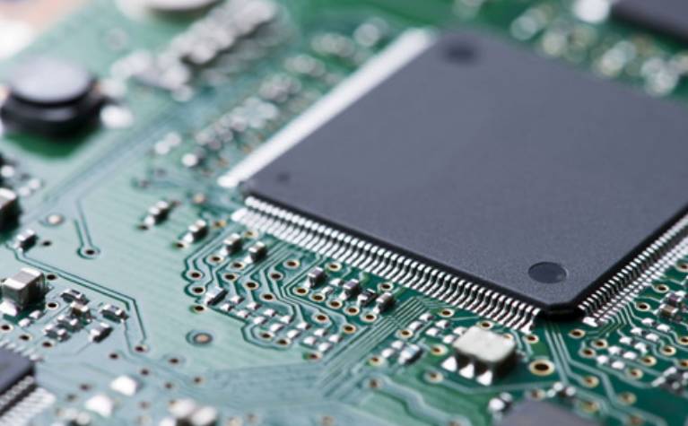
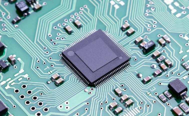
Basic inspection of PCB board
2023-03-17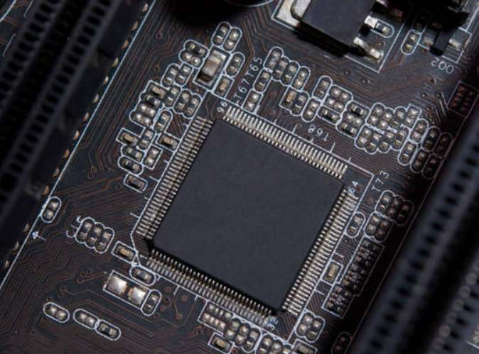


Достаточно загрузить файлы Gerber, BOM и проектные документы, и команда KINGFORD предоставит полное предложение в течение 24 часов.