
Контрактное производство электроники под ключ в Китае
Шэньчжэнь, район Баоань, улица Фуюн, улица Фуцяо, район 3, промышленный парк Лонгхуй 6

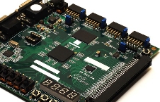
We know that the packaging of electronic devices is very important for the application of electronic technology. Packaging not only plays a role in protecting the chip and enhancing the thermal conductivity, but also serves as a bridge between the internal world of the chip and the external circuit, and integrates common functions through rational structural design. In many packaging methods, ceramic circuit board has gradually developed into a new generation of integrated circuit and power electronic module of the ideal packaging substrate, among them, ceramic substrate metallization process is a very important link in the production of ceramic circuit board, we often hear the "thick film circuit ceramic substrate" and "thin film circuit ceramic substrate" is the use of two kinds of process metallized ceramic circuit board products.
So what's the difference between the two?
First of all, they are used to make integrated circuits. Integrated circuits form passive networks and interconnect active devices on (or within) individual substrates with specific processes, thus forming micro electronic circuits so that electronic devices can play an effective role.
Integrated circuit process is the circuit required by the transistor, diode, resistor and capacitor components with a certain process in a small piece of semiconductor wafer, glass or ceramic substrate, and then with appropriate technology for interconnection, and then packaged in a shell, so that the volume of the entire circuit is greatly reduced, the number of lead lines and welding points is also greatly reduced. Integration was conceived in the late 1950s and early 1960s using silicon plane technology and thin and thick film technology.
The difference between thick film circuit and thin film circuit ceramic substrate is that they use thick film and thin film technology respectively to complete the integrated circuit on the ceramic substrate.
Relative to the three-dimensional block material, the so-called film, because of its thickness and size is relatively small, generally can be regarded as the two-dimensional form of matter. The thick film is made by rolling method. The thick film can be made independently without matrix. The thickness is usually 10~25μm. The film is formed by the accumulation of the components of the film. The film can only be attached to the matrix, and the thickness is usually about 1μm.
First, the main function of the membrane is divided into three kinds: electrical connection, component loading, surface modification.
1. Electrical connection.
The circuit board and the film are integrated with the substrate, and the components are mounted on the substrate to connect with the conductor terminal;
2. Component loading.
The chip loading on the packaging substrate requires a welding plate, while the component loading on the substrate depends on the conductor terminal. The welding plate and conductor terminal are both important parts of the membrane circuit.
3. Surface modification.
Through the use of membrane, the material can be modified in some properties, such as increasing the wear resistance, corrosion resistance, high temperature resistance and so on.
First, thick film technology
Thick film technology is a method of directly depositing slurry on substrate through micro-flow direct writing technology such as screen printing, micro straight writing technology and inkjet printing technology, and sintering at high temperature to form conductive lines and electrodes. This method is suitable for most ceramic substrates. After the material is burned at high temperature, it will form a firm adhesion film on the ceramic circuit board. After repeated many times, it will form a multilayer interconnected structure containing a resistor or capacitor circuit.
Thick film technology process flow
The slurry is mainly composed of functional phase, bonding phase and carrier.
According to different situations, the material of the functional phase is also different: as a conductor slurry, the functional phase is mostly precious metal or a mixture of precious metals; As a resistance slurry, the functional phase is conductive metal oxide; As the medium, the functional phase is mostly glass or ceramic. The functional phase determines the electrical and mechanical properties after film formation, so the material requirements are strict.
The bonding phase is mostly glass, metal oxides and composite materials of glass and metal oxides. As the name suggests, the role of the bonding phase is to bond the sintering conjunctiva to the substrate. Different from the powder state of functional phase and bonding phase, the carrier is the solution of polymer in organic solvent, which affects the process characteristics of thick film and is often used as a temporary binder for printing film and drying film.
With the development of miniaturization in electronic and electrical industry, the assembly density and wiring density of thick film circuit are required to increase continuously, which requires thinner conductor lines and narrower line spacing. Screen printing is the most widely used in thick film technology. The advantages of this technology are simple, but the disadvantages are also obvious: limited by the size of conductive paste and screen, the minimum wire width of the prepared wire is difficult to be less than 60μm, and can not make three-dimensional graphics, so it is not suitable for the production of small batch, fine circuit board. Although micro-straight writing technology and inkjet printing technology can deposit high-precision conductive graphics, they require high viscosity of slurry and are prone to channel blockage. In addition, the conductive circuit formed by thick film technology has poor electrical performance and can only be used in electronic devices with low power and size requirements.
Two, film technology
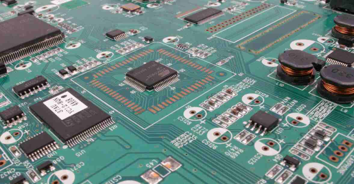
Thin film technology is a wafer-scale manufacturing technology, which is the main method of metal film deposition in microelectronics manufacturing. The ceramic circuit board was prepared by thin film technology. Firstly, a 200-500nm Cu layer was deposited on the ceramic surface by surface deposition processes such as evaporation and magnetron sputtering, so as to facilitate the subsequent electroplating process. Then, through the film, exposure, development and other processes to complete the pattern transfer, then electroplating to increase the Cu layer to the required thickness, and finally through the film removal, etching process to complete the production of conductive lines.
In recent years, ceramic circuit boards prepared by thin film technology have shown strong competitiveness in power type LED packaging because they can better meet the requirements of high precision and continuous reduction of line size. Thin film circuit line thin (minimum line width 2um), high precision (line width error 2um), but also because of the "fine line" not ups and downs, film circuit on the substrate surface quality requirements, so used for thin film circuit substrate purity requirements high (common is 99.6% purity of alumina), at the same time the high purity of ceramics also represents the processing difficulty and cost of the climb.
In addition, thin-film circuit can also easily use medium to manufacture multilayer circuit, because thin-film multilayer circuit has high interconnection density, high integration, can manufacture high-power circuit, the whole package structure has system-level function and other outstanding characteristics, in the field of microwave application is very competitive, especially in the field of airborne, spaceborne or aerospace. Its small size, light weight, high reliability characteristics are more prominent, is a very potential microwave circuit module (low noise amplifier, filter, phase shifter, etc.), and even the growing demand for T/R component substrate manufacturing technology.
However, compared with other types of substrate, there are still some problems such as the process using string form, relatively low yield, high manufacturing cost, limited number of manufacturing layers, and high requirements of equipment and process conditions.
Application comparison
The optical, electrical, magnetic, chemical, mechanical and thermal properties of thin film technology make it widely used in reflection coating, anti-reflection coating, optical recording medium, insulating film, semiconductor device, piezoelectric device, magnetic recording medium, diffusion barrier layer, anti-oxidation, anti-corrosion coating, sensor, micromachinery, photoelectric device heat sinking and so on. It has great applications in optoelectronic devices, thin-film sensors, solid-state sensors, thin-film resistors, electrofilms, capacitors, hybrid integrated circuits, solar cells, flat panel displays, surface acoustic wave filters, magnetic heads and so on.
Because of its high reliability and high performance, thick film technology has many applications in the automotive field, consumer electronics, communication engineering, medical equipment, aerospace, such as: Switching regulated power supply circuit, visual amplifier circuit, frame output circuit, voltage setting circuit, high voltage limiting circuit, aircraft communication, television, radar, remote sensing and telemetry systems, generator voltage regulator, electronic igniter and fuel injection system, magnetic and superconducting film devices, surface acoustic wave devices, film sensitive devices and other applications.


Достаточно загрузить файлы Gerber, BOM и проектные документы, и команда KINGFORD предоставит полное предложение в течение 24 часов.