
Контрактное производство электроники под ключ в Китае
Шэньчжэнь, район Баоань, улица Фуюн, улица Фуцяо, район 3, промышленный парк Лонгхуй 6

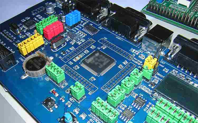
High Frequency Circuit Board is a special kind of circuit board with high electromagnetic frequency. Generally speaking, high frequency can be defined as frequency above 1GHz. Its physical properties, precision, technical reference requirements are very high, often used in vehicle collision prevention system, satellite system, radio system and other fields.
The high-frequency circuit board supplied by the new utility model is provided with a guard that can prevent the flow glue at the edge of the upper mouth and the lower mouth of the hollow groove of the core board. So, the core board and the copper coated plate placed on the upper surface and the lower surface stick in line with the frequent flow glue will not enter the hollow groove, that is, the bonding operation can be completed once pressing. Compared with the existing technology, the high-frequency circuit board which needs the secondary pressing ability to complete. The high frequency circuit plate in the new utility model has the advantages of simple structure, low cost and convenient production.
PCB preset high frequency PCB wiring techniques
First, the less the lead bending between the pins of high-speed electronic components, the better
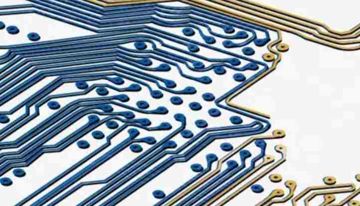
High frequency circuit wiring wire is best considered appropriate and use full straight line, demand however, can be used 45 degrees polyline or arc however, this requirement in low frequency circuit is only used to increase the copper foil fixation strength, and in high frequency circuit, satisfied with this requirement can reduce the high-frequency signal external emission and coupling between each other.
Two, high-frequency circuit components pin between the lead layer alternations less, the better
The phrase "the less interlayer alternations of leads, the better" means that the fewer holes (Via) used in the component co-signing process are the better. A pass hole can bring about 0.5pF of spread capacitance, the loss through hole number can significantly increase the rate and the possibility of loss value error.
Three, the shorter the lead between the pins of the high-frequency circuit components, the better
The radiation intensity of the signal is proportional to the length of the signal line. The longer the lead of the high-frequency signal, the easier it is to be coupled to the component close to it. Therefore, for such high-frequency signal lines as the signal time clock, crystal oscillator, DDR value, LVDS line, USB line, HDMI line, the shorter the line as possible is required.
Four, Pay attention to the "crosstalk" introduced by the signal line in the short distance running line
High frequency circuit wiring should pay attention to the "crosstalk" introduced by the signal line in the short distance running line. Crosstalk refers to the coupling phenomenon between signal lines that are not directly adjacent to each other. Because the high frequency signal along the transmission line to preach the way of electromagnetic wave transmission, signal line will play the utility of receiving antenna, electromagnetic field can + 2, 2 will be transmitted around the transmission line, signals because of the electromagnetic field coupling generated by the unwanted noise signal called Crosstalk. The parameters of PCB board layer, the distance between signal lines, the special electrical properties of the driving end and the receiving end, and the form of the end of signal lines all have a certain influence on the crosstalk. So in order to reduce the crosstalk of high frequency signals, the wiring time requirements as far as possible to do the following:
(1) If there is almost no way to prevent the horizontal running line within the same layer, in the adjacent two layers, the direction of the line must be straight for each other;
(2) Under the condition of the wiring space permit, insert a ground or the simplest surface between the two lines with more serious crosstalk, can play the utility of isolation and reduce crosstalk;
(3) When there is a time-varying electromagnetic force field in the space around the signal line, if there is no way to prevent parallel distribution, a large plane or the size of the object surface "ground" can be placed on the opposite side of the parallel signal line to greatly reduce the interference;
(4) In the digital circuit, the general time clock signal is the edge change fast signal, the external crosstalk. Therefore, in default, the clock line should be surrounded by ground lines and ground holes to reduce the spread capacitance, so reduce crosstalk;
(5) Try to use the low voltage differential timing of the clock signal of high frequency time, and pay attention to the integrity of the ground punching;
(6) On the premise of allowing wiring space, increase the spacing between adjacent signal lines, reduce the parallel length of signal lines, and try to make the clock line and the key signal line straight rather than parallel;
(7) Use the unnecessary input end do not hang in the air, but ground it or connect to the power supply (the power supply is also ground in the high-frequency signal loop), because the line suspended in the air may be equivalent to transmitting and receiving antennas, grounding can restrict the transmission. Practice has shown that crosstalk removal in this way can sometimes be effective quickly.
Five, the integrated circuit block of the power pin to increase the high frequency of lotus root capacitance
Each integrated circuit block power pin to add a high frequency dropout capacitor. Increasing the high frequency decoupling capacitance of the power pin can effectively restrict the interference of high frequency harmonics on the power pin.
Six, high frequency digital signal ground wire and analog signal ground wire to do isolation
When analog ground wire and digital ground wire are connected to the public ground wire, high frequency choke magnetic beads should be used or directly isolated and selected suitable single point interconnection. The ground potential of the ground potential of the high frequency digital signal is not exactly the same, and there is often a certain voltage difference directly between the two, and the ground wire of the high frequency digital signal is often with a very broad harmonic jack of the high frequency signal, when the direct adjacent to the digital signal ground wire and analog signal ground wire, the harmonic of the high frequency signal will be integrated through the ground wire coupling form of interference to the analog signal. Therefore, in general, the ground wire of the high frequency digital signal and the ground wire of the analog signal should be isolated. It can be considered appropriate and used in the form of single point interconnection at the appropriate position, or considered appropriate and use the form of high frequency choke magnetic bead interconnection.
Seven, prevent the loop formed by the cable
All kinds of high frequency signal wiring do not try to form a loop, if there is no way to prevent it should make the loop plane or the size of the object surface as small as possible.
PCB preset high frequency circuit board wiring note things for the item
(1) Reasonable selection of layers
When wiring the high-frequency circuit board in PCB presets, the simplest surface of the mid-waist inner layer is used as the power supply and ground layer, which can play the shielding effect. It can reduce the parasitic inductance, reduce the length of the signal line, and reduce the interleaving interference between signals. Under normal conditions, the noise of the four-layer board is 20dB lower than that of the two-layer board.
(2) Routing form
When wiring high frequency circuit boards in PCB presets, the wiring must be turned in accordance with 45° Angle, so as to reduce the transmission of high frequency signals and the coupling between each other.
(3) Cable length
When wiring high-frequency circuit boards in PCB presets, the shorter the length of the wires, the shorter the parallel distance between the two wires, the better.
(4) The number of holes
When wiring high frequency circuit boards in PCB presets, the fewer holes the better.
(5) Direction of interlayer wiring
When wiring high frequency circuit boards in PCB presets, the direction of wiring between layers should be straight, that is, the top layer is horizontal direction and the bottom layer is straight direction, so as to reduce the interference between signals.
(6) Apply copper
When wiring high frequency circuit boards in PCB presets, adding grounded copper can reduce the interference between signals.
(7) Parcel the land
In the PCB preset to the high frequency circuit board wiring, the closed signal line implementation of package disposal, can significantly increase the anti-interference experience of the signal, of course, can also be implemented on the interference source package disposal, so that it can not interfere with other signals.
(8) Signal cable
When wiring high-frequency circuit boards in PCB presets, signal wiring should not be looped, and should be routed in Daisy chain form.
(9) Decoupling capacitance
When wiring high frequency circuit boards in PCB presets, the decoupling capacitor is straddled at the power end of the integrated circuit.
(10) High frequency choke
When wiring high frequency circuit boards in PCB presets, high frequency choke components should be connected when connecting common ground cables such as digital ground and analog ground, which are usually high frequency ferrite gas magnetic beads with wires through the core hole.
How to manage the assembly line
2023-02-12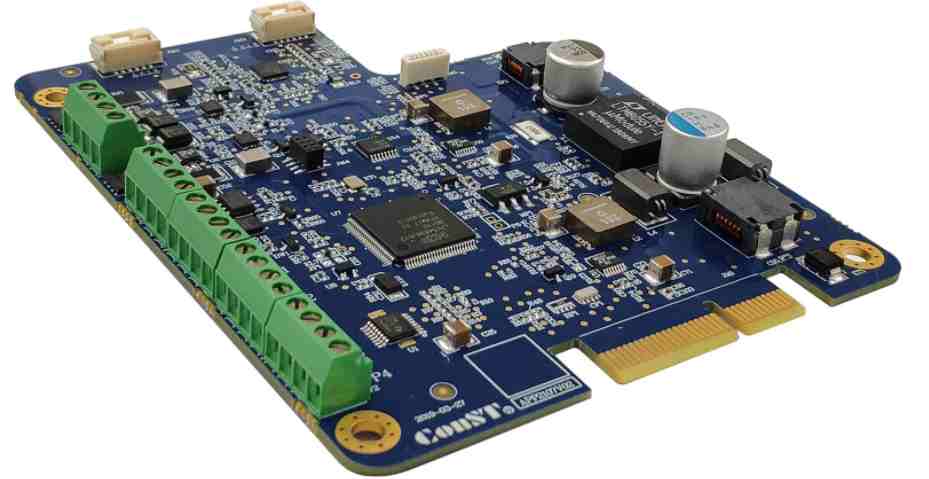


Достаточно загрузить файлы Gerber, BOM и проектные документы, и команда KINGFORD предоставит полное предложение в течение 24 часов.