
Контрактное производство электроники под ключ в Китае
Шэньчжэнь, район Баоань, улица Фуюн, улица Фуцяо, район 3, промышленный парк Лонгхуй 6

Nowadays, SMT patch technology has been effectively applied in many electronics factories, and its development prospect and direction has become the focus of attention of many people in the industry. So, in the end SMT patch processing prospects? Today, this article for you to say SMT SMT processing prospects and the main development direction. The following patch processing manufacturer Xiaobian to talk about the prospect of smt patch processing and how to patch processing PCB design related knowledge.
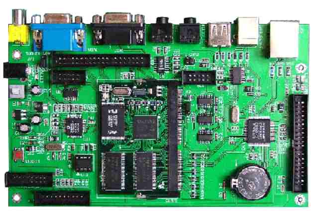
1. How to design PCB for SMT patch processing
1. First determine the function of electronic products, performance indicators, cost and overall dimensions of the overall goal of new product development and design, the first to product performance, quality and cost positioning. In general, any product design requires trade-offs and trade-offs between performance, manufacturability and cost. Therefore, the first step in the design is to define the product's purpose and grade.
2. Electrical principle and mechanical structure design, according to the structure of the whole machine to determine the size and structure shape of PCB. Draw the SMT printed board outline process diagram, mark the PCB length, width, thickness, structural parts, assembly hole position, size, leave the edge size, so that the circuit designer can carry out wiring design in an effective range.
3. Determine the process plan (1) Determine the form of assembly The selection of the form of assembly depends on the type of components in the circuit, the size of the circuit board and the equipment conditions of the production line. The selection principle of printed board assembly form: follow the principle of optimizing process, reducing cost and improving product quality

2. What is the prospect of smt patch processing
As we all know, in the future, there will be not only the combination of hardware and software, but also the combination of artificial and intelligence. In the future, based on big data, cloud computing, ICT and other foundations, the formation scale and collaboration of many platforms will change. In particular, if enterprises want to achieve resource intelligence by reducing costs and improving efficiency, they will need high-tech technology. The emergence of SMT technology has fundamentally solved the problems existing in the past and become an important milestone in the development of modern electronics.
Future development trend of SMT factor patch
First, low cost to reduce the cost is what any enterprise wants to see, but for many industries, it is difficult to reduce the cost under the premise of ensuring the quality. It is different with SMT technology, which not only aggregates resources, but also configures and connects them together, which has a positive impact on enterprise development.
The design and coordination of SMT process has a very important impact on the production of enterprises. The combination of equipment automation, rationalization of management and humanization of software will improve the production efficiency.
High quality Electronic products produced through SMT not only have good quality, excellent performance, but also have higher competitive advantages in the market.
SMT patch processing is promising
Throughout the current production of electronic products, the future SMT patch processing prospects must be very considerable. Especially under the influence of the Internet platform, high-tech products are more likely to get everyone's attention. In addition, in the era of big data, the impact of resource integration, economic sharing, pattern sharing and other ways will make SMT patch processing develop faster and better. However, because SMT patch processing has a good prospect, many people pay attention to it, so more and more enterprises join this team and want to engage in related work. And for this point, the industry also said that the SMT patch processing competition is much more fierce than before, especially some technology not pass, strength is not strong small companies, it is difficult to have a greater development in the market, want to further win, it is necessary to constantly improve technology, integrate resources.
What is the price of SMT patch?
A lot of people think that they do a small order, a small quantity, should be cheap, but it is not. Because no matter the size of the order, the early start-up work is the same, so even small batches will be charged for engineering. The final charge for patch processing will also be determined according to the size, number, complexity and process requirements of the product. Generally speaking, SMT patch processing prospects are good, although there is competition in them, but compared with the market opportunities, it is still very small. As a member of the market economy, no matter inside or outside the industry, we must have a full understanding of SMT, so that we can better grasp this technology, use this technology, so that SMT can better provide convenience for human economic development.
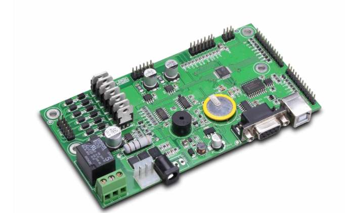
3. How to make pcb printing
So how to do double PCB copy board? The Meda engineers say that with two or more years of experience working on board designs, the design of a double-layer solution is not too difficult. You can divide the circuit board into stacked structures. In order to better design the scheme, it is better to take the substrate as the core, spread symmetrically to both sides, and separate the adjacent data signal layers by electricity.
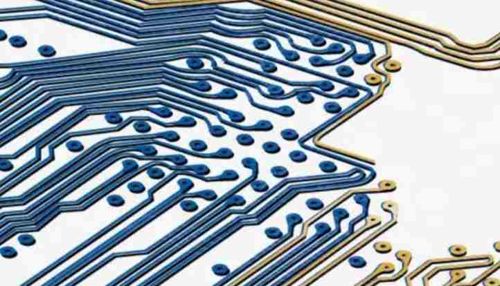
For coaxial transmission lines, top. Microstrip line solid model was used for the bottom layer and strip line solid model was used for the internal data signal layer. Data signal layer on both sides of 6 /10 /14 /18 base steel plate. It is better to use mobile phone software simulation, more inconvenient. If there are other switching power sources, the preferred choice is to walk the bold line in the data signal layer, so as not to slice the electrical geological structure. Secondly, learn the main parameters (thermal conductivity, graphic boundary, copper thickness, plate thickness) from SMT manufacturers to facilitate impedance matching. This main parameter does not need to be calculated by itself (forget it will not work, SMT patch processing manufacturers may not be able to guarantee), should be presented by the patch processing factory. With this primary parameter, you can measure the graph boundaries, line spacing (3W), and line length, and then you can take the next step. The actual multilayer plate has three kinds of buried hole, buried hole and through hole, which can be convenient to route, but the price is expensive.
Sometimes the thickness of the plate must be reduced to facilitate the insertion of PCI slot, and the material material of the insulation layer does not meet the requirements (unless it is imported from smuggled goods). In this case, the non-symmetrical plate can be selected according to the situation, such as: 14 layers in the middle and 2 layers along the edge. High speed line. Good to go inside, top. The bottom is very easy to suffer from external temperature, ambient humidity, gas hazards, not easy to smooth. If it must be detected, it can be detected through the hole. Please do not have the imagination of flying line, secant line, because the line is inside and high frequency, can not fly, line is very dense can not punch. You need to think carefully about the wiring. The way of double-layer PCB copying board is introduced here in detail. Whether it is single, two-layer PCB copying board, or double-layer copying board, we must be careful and careful in the usual work. In addition, there is another one that is bold, to actively try, more hands-on ability, so as to be able to. To get on with the task at hand.


Достаточно загрузить файлы Gerber, BOM и проектные документы, и команда KINGFORD предоставит полное предложение в течение 24 часов.