
Контрактное производство электроники под ключ в Китае
Шэньчжэнь, район Баоань, улица Фуюн, улица Фуцяо, район 3, промышленный парк Лонгхуй 6


At the beginning of a new design, because most of the time is spent on circuit design and component selection, the PCB layoutand wiring stage is often due to lack of experience, not thoughtful enough.
Failure to provide sufficient time and effort for the PCB layout and wiring phase of the design can lead to problems in the manufacturing phase or functional deficiencies as the design moves from the digital domain to the physical reality.
So what is the key to designing a circuit board that is realistic on paper and in physical form? Let's explore the first six PCB design guidelines you need to know when designing a manufacturable, functional PCB.

1 Fine tune your component layout
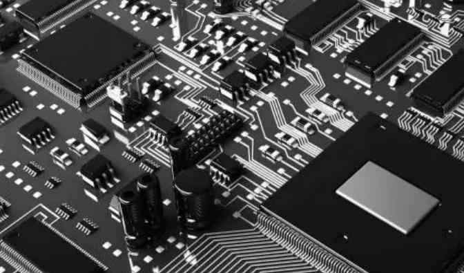
The component placement phase of the PCB layout process is both a science and an art, requiring strategic consideration of the major components available on the board. While the process can be challenging, the way you place your electronic components will determine how easy your board is to make and how well it meets your original design requirements.
While there is a general general sequence for component placement, such as sequential placement of connectors, PCB mounting devices, power circuits, precision circuits, critical circuits, etc., there are some specific guidelines to keep in mind, including:
Orientation - Ensuring that similar components are positioned in the same direction will help achieve an efficient and error-free welding process.
Layout - Avoid placing smaller components behind larger components, which may cause mounting problems due to welding of larger components.
Organization - It is recommended to place all surface mount (SMT) components on the same side of the board and all through-hole (TH) components on top of the board to minimize assembly steps.
One final PCB design guideline to note - when using mixed technology components (through hole and surface mount components), the manufacturer may require additional processes to assemble the board, which will increase your overall cost.
2 Power supply, grounding, and signal cabling are properly placed
After placing the component, you can next place power, ground, and signal wiring to ensure a clean trouble-free path for your signal. At this stage of the layout process, keep the following guidelines in mind:
Locate the power supply and grounding plane
It is always recommended that the power supply and ground plane layers be placed inside the board while remaining symmetrical and centered. This helps prevent your circuit board from bending, which is also related to whether your components are positioned correctly.
For supplying power to the IC, it is recommended to use a common channel for each power channel, ensure a strong and stable cable width, and avoid Daisy chain power connections from component to component.
Signal cables are connected through cables
Next, connect the signal wires as designed in the schematic diagram. It is recommended to always take the shortest possible path and direct path between components.
If your component needs to be fixed horizontally without deviation, it is recommended to route the circuit board basically horizontally where the component exits, and then vertically after the exit.
This keeps the element in place horizontally as the solder moves through the weld. As shown in the top half of the figure below. The signal routing mode in the lower part of the figure below may cause component deflection with the flow of solder during welding.
Define network width
Your design may require different networks that will carry a variety of currents, which will determine the desired network width. Given this basic requirement, a 0.010 "(10mil) width is proposed for low current analog and digital signals. When your line current exceeds 0.3 amps, it should be widened. There is a free line width calculator to make this conversion process easy.
You may have experienced how large voltage and current spikes in the power supply circuit can interfere with your low-voltage current control circuit. To minimize such interference problems, please follow the following guidelines:
Isolation - Ensure that each circuit of power is kept power and control separate. If you must connect them together in the PCB, make sure it is as close to the end of the power path as possible.
Layout - If you have placed a ground plane in the middle layer, be sure to place a small impedance path to reduce the risk of interference from any power circuits and to help protect your control signals. You can follow the same guidelines to keep your digital and analog separate.
Coupling - To reduce capacitive coupling due to placing large ground planes and running lines above and below them, try to cross analog ground only through analog signal lines.


Достаточно загрузить файлы Gerber, BOM и проектные документы, и команда KINGFORD предоставит полное предложение в течение 24 часов.