
Контрактное производство электроники под ключ в Китае
Шэньчжэнь, район Баоань, улица Фуюн, улица Фуцяо, район 3, промышленный парк Лонгхуй 6

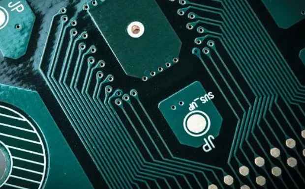
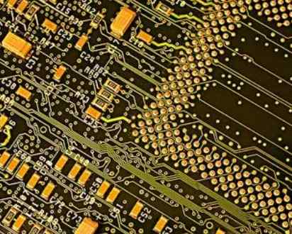
It can be said that pcb routing is the most important and time-consuming process in the entire PCB design. Here we share some pcb routing principles.
1. Layered wiring: Separate the power supply and load parts of the power supply to avoid mutual interference and improve the signal-to-noise ratio.
2. Appropriate increase of ground copper: Ground copper can effectively reduce electromagnetic interference, so it can be appropriately increased in the power supply.
3. Choose the right line width: according to the size of the current and the length of the distance, choose the right line width to ensure the safety and stability of the circuit.
4. Pay attention to the wiring near the voltage regulator chip: Place the filter capacitor and noise reduction capacitor near the voltage regulator chip to ensure the stability of the power supply.
5. Separate wiring: Separate the input and output power cables to avoid interference with input signals.
6. Eliminate loops: When arranging power cables, ensure that no loops are formed to prevent noise.
7. The closer the wiring distance is, the better: the distance of the power wiring is reduced as far as possible, which helps to reduce the interference of the power supply fluctuation on the circuit.
8. Symmetrical wiring: When arranging the power line, the symmetrical layout should be ensured as far as possible to avoid interference and circuit stability problems.
9. Power line length as short as possible: the power line as short as possible will reduce the degree of noise and modulation interference, thus improving the stability and performance of the circuit.
10. Solid ground cable connection: The ground cable of the power supply must be firmly and reliably connected to ensure normal grounding operation.
11, the capacitance of the bypass porcelain capacitor can not be too large, and its parasitic series induction is as small as possible, multiple capacitors in parallel can improve the impedance characteristics of the capacitor;
12. The parasitic parallel capacitance of the inductor should be as small as possible, and the distance between the inductor pin pad should be as far as possible;
13. Avoid placing any power or signal wiring on the formation;
14. The area of high-frequency loop should be reduced as much as possible;
15, hole placement should not destroy the path of high frequency current on the formation;
16. A small circuit on the system board needs different ground connection, and the ground connection of the small circuit is connected with the ground connection of the power supply through a single point;
17, control chip to the upper and lower end of the field effect tube drive circuit loop should be as short as possible;
18, switching power circuit and control signal circuit components need to be connected to the small ground, the two strata are generally connected through a single point.
19. In PCB wiring, it is inevitable to turn the wire. When the right Angle of the wire appears, extra parasitic capacitance and parasitic inductance will be generated at the corner. PCB design should avoid sharp Angle and right Angle, produce unnecessary radiation, at the same time PCB production process performance is not good.
20. The direction of the adjacent plane is orthogonal. Avoid running different signal lines in the same direction on adjacent floors to reduce unnecessary cross-talk between floors

Solve the heat problem
Have you ever experienced circuit performance degradation or circuit board damage due to heat problems? As a result of not considering the heat dissipation, there have been many problems plaguing many designers. Here are some guidelines to keep in mind to help solve heat dissipation problems:
Identify troublesome components
The first step is to start thinking about which components dissipate the most heat from the board. This can be done by first finding the "thermal resistance" rating in the element's data sheet and then following the recommended guidelines to transfer the heat generated. Of course, radiators and cooling fans can be added to keep components cool, and remember to keep key components away from any high heat sources
Add hot air pad
The addition of hot-air pads is useful for manufacturing fabricable circuit boards, and they are critical for applications of wave soldering on high copper content components and multilayer circuit boards. Because of the difficulty in maintaining process temperature, it is always recommended to use hot-air pads on through-hole elements to make the welding process as simple as possible by slowing down the rate of heat loss at the element pins.
As a general rule, always use hot air pad connections for any through or through holes connected to the ground plane or power plane. In addition to the hot air pad, you can also add teardrops where the pad connects the wires to provide additional copper foil/metal support. This will help reduce mechanical and thermal stress.
Reflection to crosstalk after PCB design
2023-03-21


Достаточно загрузить файлы Gerber, BOM и проектные документы, и команда KINGFORD предоставит полное предложение в течение 24 часов.