
Контрактное производство электроники под ключ в Китае
Шэньчжэнь, район Баоань, улица Фуюн, улица Фуцяо, район 3, промышленный парк Лонгхуй 6


1.BGA welding spots are all concentrated below the body, after welding it is difficult to use visual or AOI(Auto OpticalDetect) image detector for quality detection, and welding is more difficult. Sometimes, even with X-rays, it is difficult to tell if there is gas welding or fake welding. Some rotated-angle X-rays or 5DX have the opportunity to check for BGA gas welding problems, but such X-ray detectors are expensive and do not appear to have reached the economic scale of online testing and mass production.
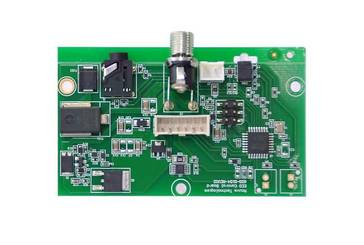
SMT patch processing
Experience shows that the most important quality problems after BGA welding are almost concentrated on HIP(headrest effect, pillow effect, double ball effect). This is because when the circuit board (PCB) passes through the high temperature area of reflow welding, it is easy to cause the deformation of the PCB board and BGA body, and when the solder paste and BGA ball melt into a liquid, they separate from each other without contact. When the temperature of the circuit board begins to drop and below the melting point of the solder, the deformation of the PCB and BGA body becomes smaller, but the solder paste and the solder ball have been condensed into a solid state, there is a fake welding phenomenon of double ball lap, namely the so-called hot isostatic pressing (HIP).
Because the diagonal of BGA package is the longest, the relative deformation is the most serious, and more than 90% of the HIP appears in the outermost tin ball of BGA or its four corner point area. oem has a group of high-quality management personnel and skilled staff, and has the international advanced level of production equipment and complete testing technology and scientific quality management system, is committed to meet the OEM manufacturers/customers of different types of manufacturing requirements, to provide a full range of services from product components procurement to production assembly, technical support. The second largest area of deformation is the outermost tin ball in the BGA. Based on the above experience and a large number of experiments conducted by SMT predecessors, it is shown that increasing the filler metal content of BGA can effectively reduce the thermal isostatic pressure (HIP) problem caused by temperature. However, it should be noted that if the amount of solder paste is increased too much, it will lead to the problem of short circuit welding.
Therefore, the method chosen below is to locally increase the number of solder paste in BGA, rather than all the solder balls and pads.
To change the amount of solder paste BGA can start from the steel plate (screen), the basic principle is to let BGA tin ball of the outermost or four corners of the solder paste printing, than the remaining number of the tin ball solder paste is not much, but not much more than the rest of the tin ball solder paste, the basic principle is to let the outer row of the tin ball or four corners of the solder paste printing, than the remaining number of the tin ball solder paste, But not too much. Only in this way, when the PCB and BGA body deformation, the solder paste can maintain adequate contact with the tin ball under the BGA.
Is selected by locally increasing the amount of tin paste in the BGA, not by increasing the amount of tin in all ball pads.
When the BGA tin ball is greater than 0.4mm:, the printing amount of the solder paste around the BGA is increased, and the steel plate is opened into a square, forming an inner ring with the original tin ball circular pad. The original quantity of other balls and pads shall be maintained.
When the BGA solder ball is less than 0.4mm:, the four sides of the external BGA paste printing remains unchanged, but the other internal tin balls reduce the amount of paste. oem has a group of high-quality management personnel and skilled staff, and has the international advanced level of production equipment and complete testing technology and scientific quality management system, is committed to meet the OEM manufacturers/customers of different types of manufacturing requirements, to provide a full range of services from product components procurement to production assembly, technical support. Open the steel plate into a square, then use the original tin ball round pad to form an outer ring.
Thus, regardless of the size of the BGA, the amount of tin paste in the outermost circle of the tin ball will be about 16.7% more than that in the inner circle. Used to ensure PCB and BGA body flow through high temperature deformation, there is enough solder paste to maintain contact with the tin ball under the BGA.
2. How does the SMT patch factory clean PCB after surface mounting and welding
Every time an electronic product is welded, flux or other types of contaminants can be left on the surface of the PCB (printed circuit board), even if a halogen-free cleaning flux is not used. In my experience, never put too much trust in "unclean". In short, the cleaning of PCB after surface mount welding plays a crucial role in ensuring the reliability, electrical function and service life of electronic products. This article will discuss the importance of cleaning after surface mounting and welding, and list some common cleaning methods.

Significance of PCB cleaning after surface mounting welding The following aspects can fully explain the importance of PCB cleaning after surface mounting welding:
PCB cleaning after surface mounting and welding can prevent electrical defects.
Of all the electrical defects, leakage is the most prominent, which is the fundamental factor that reduces the long-term reliability of PCB boards. This type of defect is mainly caused by ionic contaminants, organic residues and other adhesive substances left on the board surface.
PCB cleaning after surface mount welding can eliminate corrosive substances. Erosion can damage the circuit and cause brittle components or devices. Corrosive substances can conduct electricity in a humid environment, which will further cause short circuit or even failure of PCB board. Eliminating corrosive substances actually removes negative factors that hinder the long-term reliability of PCB boards.
PCB cleaning after surface mounting and welding can make the appearance of the circuit board clear.
Surface mount PCB board clean after welding has a clear appearance, exposing some defects for easy inspection and troubleshooting, such as heat damage and lamination.
Source analysis of pollutants
The white contaminant left on PCB board surface after welding has a complex composition. They can be flux, oxide or flux and metal reagents, welding masks and PCB laminating materials. In addition to the above substances, the production of white contaminants is related to other elements, including PCB design, SMT technology (such as reflow soldering time and temperature), temperature and humidity.
classification of PCB cleaning methods after surface mount welding
Manual cleaning method:
The acetone solution is used to soak the PCB board for about 10 minutes. Then, use a railing brush to remove contaminants from the solder joints in the ethanol solution. Next, remove the plate 3 minutes before washing with deionized water. After that, anhydrous ethanol is used for dehydration. Finally, a nitrogen gun is used to dry the surface of the plate until no water marks are visible.
In the process of manual cleaning, the use of high solubility of acetone soaked circuit board, can effectively dissolve pollutants in the solution. The circuit board is then physically scrubbed by placing the circuit board in ethanol and brushing away fine flux contaminants. Next, the organic solvent must be dehydrated with the help of deionized water. Finally, nitrogen was used to dry the board surface so that manual cleaning could be done after surface mount soldering. The process can be summarized in the following figure.
ultrasonic cleaning method:

Acetone solvent is used for ultrasonic cleaning methods. First, the PCB board was immersed in acetone solvent for 10 minutes. It is then placed in a quartz container dedicated to absolute ethanol, in which the circuit board is impregnated. Next, ultrasonic cleaning is performed after placing the quartz container in the ultrasonic cleaning tank. The ultrasonic cleaning lasted for 5 minutes with the ultrasonic power of 240W, and then the quartz container was removed with a basket after the ultrasonic cleaning switch was turned off. Then, wash with deionized water for 5 minutes and dehydrate the circuit board with anhydrous ethanol. Finally, nitrogen gas is used to dry the surface.
During the ultrasonic cleaning process, the circuit board is placed in the ethanol agent, which is different from manual cleaning. Based on the principle of ultrasonic vibration, ultrasonic cleaning is designed to remove flux residue and dehydrate through deionized water. Finally, it enters the drying stage with the help of nitrogen gas. The whole process of ultrasonic cleaning is shown in the figure below.
Gas phase cleaning method:
The device condensing system is turned on first and allowed to run for 5 to 10 minutes. Then, turn on the device heating system and heat the cleaning agent to boiling temperature. Place the circuit board in the cleaning basket, then place it in the boiling tank. Boil for 3 to 5 minutes. The basket is then placed in the steam area for steam cleaning for 3 to 5 minutes. Then, spray the surface of the circuit board with cleaner for 10 to 20 seconds. After that, place the basket slightly in the rinse tank for 1 to 2 minutes. Finally, the basket is removed after the reagent is completely volatilized through the condensation drying device.
When the PCB board is put into the thermal steam, the hot steam will condense on the surface of the circuit board with a cooler surface, resulting in the dissolution of the grease and dirt on the surface of the PCB compone-nts. The dissolved grease and dirt is dipped into the boiling agent while steam accumulates on the condensate coil around the boiling agent. The steam will return as a liquid to the separation chamber, which can be recirculated with the separated water and impurities filtered. The principle of chemical gas phase cleaning is shown in the figure below.

The comparison of all cleaning methods, by observing the PCB wiring and surface conditions, and by comparing the manual cleaning, ultrasonic cleaning and gas phase cleaning methods on the PCB after surface mounting and welding, it can be concluded that the organic solvent cleaning can completely clean the flux residue from the PCB surface. However, manual cleaning and ultrasonic cleaning can sometimes still leave flux residue on certain parts of the PCB board. Therefore, the comprehensive analysis concludes that the organic solvent cleaning equipment should have higher reliability, lower toxicity and higher safety, so as to make the cleaning more thorough, produce better cleaning effect.
In summary, electronic assembly capabilities are not limited to the scope of manufacturing and assembly technology. However, as far as board welding and soldering PCBS are concerned, flux electronics are also an unavoidable aspect, which plays a crucial role in determining the reliability and functionality of the final electronic product


Достаточно загрузить файлы Gerber, BOM и проектные документы, и команда KINGFORD предоставит полное предложение в течение 24 часов.