
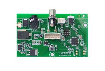
Контрактное производство электроники под ключ в Китае
Шэньчжэнь, район Баоань, улица Фуюн, улица Фуцяо, район 3, промышленный парк Лонгхуй 6

PCB wiring is very important in the whole pcb design, how to do fast and efficient wiring, and let your PCB wiring look tall, is worth studying. Sorted out the PCB wiring needs to pay attention to 7 aspects, quick to check the gaps!
How can PCB wiring become better
1. Common ground processing of digital circuit and analog circuit
There are now many PCBS that are no longer single-function circuits (digital or analog), but consist of a mix of digital and analog circuits. Therefore, it is necessary to consider the interference between them when wiring, especially the noise interference on the ground wire. The digital circuit has a high frequency and the analog circuit has a strong sensitivity. For the signal line, the high frequency signal line is far away from the sensitive analog circuit devices as far as possible. For the ground wire, the rectifier PCB has only one node to the outside world, so the problem of number and mode common ground must be handled inside the PCB, and the digital and analog ground are actually separated from each other in the board. Only at the interface (such as plug, etc.) between PCB and the outside world. There is a little bit of short circuiting between digital and analog, but note that there is only one connection point. There are also differences on the PCB, which is determined by the system design.
2. The signal cable is distributed on the electrical (ground) layer
In the multi-layer printed board wiring, because in the signal line layer is not finished the line is not much, and then more layers will cause waste will also increase the production of a certain amount of work, the cost is increased accordingly, in order to solve this contradiction, you can consider wiring on the electrical (ground) layer. The power layer should be considered first and the formation second. Because it's better to preserve the integrity of the formation.
3. Processing of connecting legs in large area conductors
In a large area of grounding (electricity), the legs of commonly used components are connected to it, and the treatment of the connecting legs needs comprehensive consideration. In terms of electrical performance, the welding pad of the component leg is fully connected with the copper surface, but there are some bad hidden dangers for the welding assembly of the components, such as: ① welding requires a high-power heater. (2) easy to cause virtual solder joints. Therefore, taking into account the electrical performance and process needs, make a cross welding pad, called heat shield, commonly known as Thermal pad (Thermal), so that when welding due to excessive heat dissipation section and the possibility of virtual solder joint greatly reduced. The electrical connection (ground) leg of the multilayer plate is treated the same
4. The role of network system in wiring
In many CAD systems, the wiring is determined by the network system. Although the grid is too dense, the path is increased, but the step is too small, the amount of data in the graph field is too large, which inevitably has higher requirements for the storage space of the equipment, but also has a great impact on the computing speed of the object computer electronic products. Some paths are not valid, such as those occupied by the pad of the component leg or by the mounting holes, fixing holes, etc. Too sparse grid and too few channels have great influence on the propagation rate. So there should be a reasonable grid system to support the wiring. The distance between the legs of a standard component is 0.1 inch (2.54mm), so grid systems are generally based on 0.1 inch (2.54mm) or integral multiples less than 0.1 inch, such as 0.05 inch, 0.025 inch, 0.02 inch, etc.

5. Processing of power supply and ground wire
Even if the wiring in the whole PCB board is completed very well, but because of the power supply, ground wire is not thoughtful and caused by interference, will make the performance of the product decline, sometimes even affect the success rate of the product. So the wiring of the power supply and ground wire should be taken seriously, the noise interference generated by the power supply and ground wire should be reduced to a minimum to ensure the quality of the product. For every engineering personnel engaged in the design of electronic products will understand the cause of the noise between the ground and the power line, now only to reduce the noise suppression is described: it is well known that between the power supply and the ground to add the coupling capacitance. Try to widen the width of the power supply and ground wire, it is best that the ground wire is wider than the power cable, their relationship is: ground wire "power cable" signal cable, usually signal cable width: 0.2 ~ 0.3mm, the most fine width can reach 0.05 ~ 0.07mm, the power cable is 1.2 ~ 2.5 mm. The PCB of digital circuit can be composed of a wide ground wire circuit, that is, to form a ground network to use (the ground of analog circuit can not be used in this way) with a large area of copper layer as ground, in the printed board is not used to connect with the ground as ground. Or made of multilayer board, power supply, ground wire each occupy a layer.
6. Design Rule Check (DRC)
After the wiring design is completed, it is necessary to carefully check whether the wiring design conforms to the rules formulated by the designer, and also confirm whether the rules formulated meet the requirements of the printed board production process. The general inspection includes the following aspects: Whether the distance between wire and wire, wire and component pad, wire and through hole, component pad and through hole, through hole and through hole is reasonable, whether it meets the Production requirements. Are the cords and ground wires of appropriate width, and are there tight coupling (low wave impedance) between the power supply and ground wire? Is there any place in PCB where the ground wire can be widened? Are optimal measures taken for critical signal lines, such as minimum length, protected lines, and clearly separated input and output lines. Analog circuit and digital circuit parts, whether there are independent ground. Whether the graphics (such as ICONS, marking) added to the PCB will cause signal short circuit. Modify some lines that are not ideal. Is there a process line on the PCB? Whether the solder resistance meets the requirements of the production process, whether the solder resistance size is appropriate, whether the character mark is pressed on the device pad, so as not to affect the quality of the electrical equipment. Whether the outer frame edge of the power layer in the multilayer panel is reduced, such as the copper foil of the power layer exposed outside the panel, it is easy to cause short circuit.
7. Design of through hole (via
Through hole (via) is one of the important components of multilayer PCB, the cost of drilling usually accounts for 30% to 40% of the PCB board. Simply put, every hole in the PCB can be called a pass hole. From the point of view of function, the hole can be divided into two categories: one is used as an electrical connection between the layers; The second is used for fixing or positioning devices. In terms of technological process, through holes are generally divided into three categories, namely blind via, buried via and through via.
Blind holes are located on the top and bottom surfaces of the PCB and are of a certain depth. They are used to connect the surface circuit to the inner circuit below. The depth of the holes usually does not exceed a certain ratio (aperture). Buried holes are connection holes located in the inner layer of the PCB that do not extend to the surface of the PCB. Both types of holes are located in the inner layer of the circuit board, which is completed by a through-hole molding process prior to lamination. Several inner layers may be overlapped during the through-hole formation process. The third type, called through-holes, runs through the entire circuit board and can be used for internal interconnection or as installation positioning holes for components. Because the through hole in the process is easier to achieve, the cost is lower, so most of the printed circuit board is used in it, rather than the other two through holes. The following mentioned through holes, without special instructions, are considered as through holes.
First, from the design point of view, a hole is mainly composed of two parts, one is the middle of the drill hole (drill hole), the second is the welding pad area around the drill hole. The size of these two parts determines the size of the hole. Obviously, in the design of high speed, high density PCB, the designer always wants the hole as small as possible, the template can leave more wiring space, in addition, the hole is smaller, its own parasitic capacitance is smaller, more suitable for high speed circuit. But as hole sizes get smaller, they cost more, and don't keep getting smaller. It's limited by technology such as drill and plating. The smaller the holes, the longer it takes to drill, and the more off-center it gets. When the hole depth is more than 6 times the diameter of the hole, it is impossible to guarantee the uniform copper plating on the hole wall. For example, the thickness (through hole depth) of a normal 6-layer PCB board is about 50Mil, so the minimum drilling diameter provided by PCB manufacturers can only reach 8Mil.
The parasitic capacitance through the hole itself has parasitic capacitance to the ground. If the diameter of the isolation hole through the hole on the laying layer is D2, the diameter of the welding plate through the hole is D1, the thickness of the PCB board is T, and the dielectric constant of the substrate is ε, the parasitic capacitance through the hole is approximately: C= "1".41εTD1/ (D2-D1) The main effect of the parasitic capacitance through the hole on the circuit is to prolong the signal rise time and slow down the circuit speed. For example, for a PCB board with a thickness of 50Mil, if a through-hole with an inner diameter of 10Mil, a diameter of 20Mil of the pad is used, and the distance between the pad and the copper floor area is 32Mil, then we can approximate the parasitic capacitance of the through-hole through the above formula: C=1.41x4.4x0.050x0.020/ (0.032-0.020) =0.517pF, the rise time change caused by this part of capacitance is: T10-90=2.2C (Z0/2) =2.2x0.517x (55/2) =31.28ps. It can be seen from these values that although the effect of the parasitic capacitance of a single hole is not obvious, the designer should be careful if multiple holes are used to switch between layers in the route.
Similarly, there are also parasitic inductors in the presence of parasitic capacitance through the hole. In the design of high-speed digital circuits, the harm caused by parasitic inductance through the hole is often greater than the influence of parasitic capacitance. Its parasitic series inductance will weaken the contribution of the bypass capacitance and reduce the filtering effectiveness of the whole power system. We can simply calculate the parasitic inductance of a through-hole approximation using the following formula: L= "5".08h [ln (4h/d) +1] where L refers to the inductance of the through-hole, h is the length of the through-hole, and d is the diameter of the central borehole. It can be seen from the formula that the diameter of the through hole has little influence on the inductance, while the length of the through hole has the biggest influence on the inductance. Using the above example again, the out-of-hole inductance can be calculated as L=5.08x0.050 [ln (4x050/0.010) +1] =1.015nH. If the rise time of the signal is 1ns, the equivalent impedance is XL=πL/T10-90=3.19Ω. Such impedance can no longer be ignored in the presence of high frequency current. In particular, note that the bypass capacitor needs to pass through two holes when connecting the power layer to the formation, so that the parasitic inductance of the holes will be multiplied.
Through the above analysis of the parasitic characteristics of the holes, we can see that in the design of high-speed PCB, seemingly simple holes often bring great negative effects to the design of the circuit. In order to reduce the adverse effects brought by the parasitic effect of the hole, the design can be as far as possible:
1, from the cost and signal quality, choose a reasonable size of the hole size. For example, for the design of 6-10 layers of memory module PCB, it is better to choose 10/20Mil (drill/pad) pass hole, for some high-density small size boards, you can also try to use 8/18Mil pass hole. With current technology, it is difficult to use smaller holes. For the power supply or ground wire hole can be considered to use a larger size, to reduce the impedance.
2. From the two formulas discussed above, it can be concluded that the use of thinner PCB board is beneficial to reduce the two parasitic parameters through the hole.
3. The signal routing on the PCB board should not be changed as far as possible, that is to say, try not to use unnecessary holes.
4. The pins of the power supply and the ground should be drilled nearby. The shorter the lead between the pins and the holes, the better, because they will lead to the increase of inductance. At the same time, power and ground leads should be as thick as possible to reduce impedance.
5. Place some grounded holes near the holes of the signal changing layer in order to provide the nearest loop for the signal. You can even put a lot of extra ground holes on the PCB board. Of course, you need to be flexible in your design. The perforated model discussed above is the case that each layer has pads, and sometimes, we can reduce or even remove the pads of some layers. Especially in the case of very large pore density, it may lead to the formation of a fault slot that cuts off the circuit in the copper layer. To solve this problem, in addition to moving the position of the hole, we can also consider reducing the size of the solder pad in the copper layer.


Достаточно загрузить файлы Gerber, BOM и проектные документы, и команда KINGFORD предоставит полное предложение в течение 24 часов.