
Контрактное производство электроники под ключ в Китае
Шэньчжэнь, район Баоань, улица Фуюн, улица Фуцяо, район 3, промышленный парк Лонгхуй 6

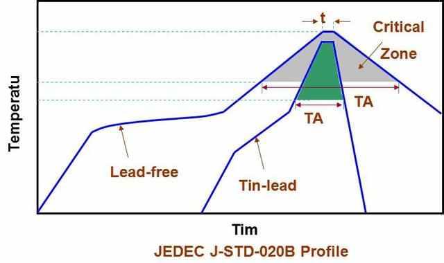
1. The traditional cleaning process will have a destructive impact on the environment, and the non-cleaning welding technology is the best way to solve this problem. Clean - free welding consists of two techniques. One is to use a low solid content no-clean flux. The other is welding inert protective gas. For the first method, flux activity is only effective for a certain period of time, and the resulting weld cannot be secured, sometimes resulting in weld defects such as bridging, tilting, and spotting, thus limiting its application areas and requiring further research. Development. For the second method, welding is performed in an inert gas, which eliminates the environment in which the welding portion is oxidized during the welding process, thus reducing or eliminating the use of flux. Prior to welding, only a small amount of weakly active flux can be used to remove oxides from the surface of the welded part and maintain an inert gas atmosphere, or the part leads can be machined to achieve surface welding.
Face welding technology is not only suitable for through hole assembly, mixed assembly and full surface assembly parts, but also suitable for multi-lead fine spacing parts assembly. The following benefits are shown in these applications.
(1) When used in double wave soldering process, welding defects caused by flux gas can be eliminated, nozzle blockage can be eliminated, and stability of wave soldering can be improved with high quality and convenience due to less or less use of flux. Weld the connection.
(2) Eliminate the cleaning process and the corresponding equipment, greatly reducing the operating cost.
(3) As the solder and the part to be welded are oxidized, the wettability of the solder and the weldability of the part to be welded are improved, thus minimizing the welding defects, greatly improving the welding quality, and ensuring the welding reliability of the parts.
Therefore, the non-cleaning welding technology is a very valuable practical technology, and its popularization and application in the technical cost and protection of human living environment has very important practical significance.
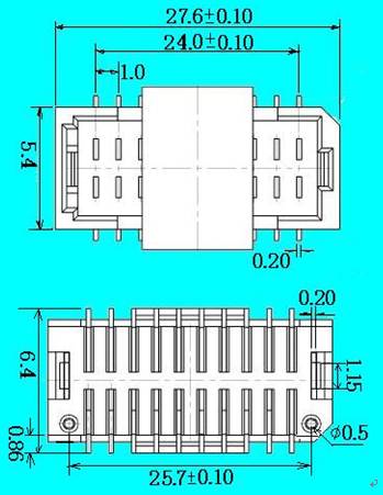
2. Suggestions on naming rules for SMT patch processing pad
(Inch IN British system: in; The metric millimeter is represented by MM, and the decimal point in the middle of the data is represented by d. The following data are some dimensional parameters of the components, which can determine the size and shape of the pad. Separate different parameters with an "X")
1. Common resistance (R), capacitance (C), inductance (L), magnetic bead (FB) class components (rectangle of component shape) : component type + size system + appearance size specification naming.
Such as: FBIN1206, LIN0805, CIN0603, RIN0402, CIN0201;
Two, discharge resistance (RN), discharge capacity (CN) : component type + size system + appearance size +P+ pin number named.
For example, RNIN1206P8. Represents the discharge resistance, the appearance specification size is 1206, there are 8 pins in total;

Iii. Tantalum capacitor (TAN) : component type + size system + appearance size specification naming.
For example: TANIN1206. Represents tantalum capacitor, its external size is 1206;
Iv. Aluminum electrolytic capacitor (AL) : component type + size system + appearance size (the diameter of the above part X component height) specification naming.
For example, ALMM 5X5d4. Represents the aluminum electrolytic capacitor, the upper part of the diameter is 5mm, the height of the element is 5.4mm;
Five, diode (DI) : here mainly refers to two electrode diode
There are two categories:
1. Planar diode (DIF) : component type + size system + pin size in contact with PCB (length X width) +X+ pin span size named.
For example, DIFMM1d2X1d4X2d8. Represents a planar diode, the length of pins is 1.2mm, the width is 1.4mm, and the span between pins is 2.8mm;
2, cylindrical diode (DIR) : component type + size system + appearance size specification name.
DIRMM3d5X1d5. Represents a cylindrical diode with an external dimension of 3.5mm in length and 1.5mm in width
Six, transistor class components (SOT type and TO type) : directly with the standard specification name.
Such as SOT-23, SOT-223, TO-252, TO263-2 (two-pin type), TO263-3 (three-pin type).
3. What preparations should be made for the smt patch factory before production
SMT patch processing from sample to mass production stage, we need to do a good job of pre-production preparation, to ensure that all materials can be successfully online, to avoid all kinds of stop-line looking accidents, because production efficiency is the lifeline of SMT patch processing plant. In order to do a good job in pre-production preparation, make it fully effective and ensure the completion on time, so the standardized production process management is particularly important. The following global technology for you to brief SMT patch processing and manufacturing must do some pre-production preparation.
I. Engineering
1. Arrange preparation 4 hours in advance according to the planned order: steel mesh, fixture review, data, procedures, material sample follow-up and completion of special requirements.
2. Test orders will be required after SMT production, and the first finished product will be tested on the same day.
3. Provide temporary ope SMT patch processing:ration plan for poorly tested and functionally defective products within 1 hour before delivery, and specific operational production measures within 1 day.
Ii. Production
1. Arrange material requisition 4 hours in advance and prepare materials according to the planned order.
2. Technicians confirm the integrity of steel mesh, fixture and data (procedures) 2 hours before wire transfer.
3. In the online production of tail plate cleaning, the technician is responsible for docking the material clerk, and the department head follows up and arranges to complete the replenishment within half an hour.
4. Visual inspection of 5PCS after intermediate inspection of furnace, defects exceeding 5%, report to technician and supervisor for analysis and treatment.
DIP plug-in processing:
1. Elongate 4 hours in advance according to the planned order, make the first piece, confirm the quality and project.
2. Elongate 4 hours in advance to determine the auxiliary materials: furnace fixture, welding fixture, tool, or guest fixture, etc.
3. Elongate the pre-production meeting (for each product), and explain the process and quality within 3-5 minutes.
4. The defective test was as high as 5%, and the production staff reported it for a long time, supervisor; At the same time, the engineering intervention analysis, within 1 hour to reply to the specific plan, production implementation, quality supervision completed.
Three. Quality
1.SMT's first IPQC wire following production; DIP, IPQC confirm the first inspection and assist production to finish 2 hours in advance.
2. Testing and assembly: According to the planned order, the quality shall be given 4 hours in advance in production and engineering, and the first part shall be confirmed by IPQC and completed within 2 hours before the production goes online.
Iv. Current process: All products need to be tested and burned
New order -- SMT -- first sample of engineering trial production -- DIP -- test -- assembly
Return order -- SMT -- DIP (first sample for production trial) -- test -- assembly
V. New Process (Optimization)
1. Reorder production tracking burning and testing
Return order -- SMT -- AOI -- DIP (first production sample) -- test -- assembly
2. Arrange preparation for production of all DIP first materials on the day after SMT of the order; Leading arrangement of welding, testing and assembly engineering.
New order -- SMT -- AOI -- first sample of engineering trial production -- DIP -- test -- assembly
The above is smt factory small editor to share, hope to help you, we undertake a variety of products smt patch processing, DIP plug-in processing, post-welding processing, assembly processing, testing, aging, assembly, contract materials, OEM OEM materials and other manufacturing services
How can PCB wiring become better
2023-02-18


Достаточно загрузить файлы Gerber, BOM и проектные документы, и команда KINGFORD предоставит полное предложение в течение 24 часов.