
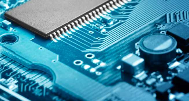
Контрактное производство электроники под ключ в Китае
Шэньчжэнь, район Баоань, улица Фуюн, улица Фуцяо, район 3, промышленный парк Лонгхуй 6


Delta LA = (180 ℃ ~ 30 ℃) x1.5 x10-5 m / ℃ X1000mm = 2.25 mm
Delta LB = (180 ℃ ~ 30 ℃) X2.5 X10-5 m / ℃ X1000mm = 3.75 mm
At this time, because the semi-curing is still in the free state, the two core plates are long and short, non-interference and deformation has not occurred.
As shown in Figure 2, the compression will be kept at high temperature for a period of time until the semi-curing is completely cured, at which point the resin becomes cured and cannot flow freely, and the two core plates are combined together. When the temperature drops, if there is no interlayer resin binding, the core plate will return to the initial length without deformation. But in fact, the two core plates have been bonded by the solidified resin at high temperature, and cannot shrink at will during the cooling process. Core plate A should shrink by 3.75mm When the force is balanced, the B-core plate cannot shrink to 3.75mm, while the A-core plate shrinks to more than 2.25mm, thus making the whole plate bend in the direction of B-core plate, as shown in Figure 2.
According to the above analysis, it can be seen that whether the laminated structure and material type of PCB boardare evenly distributed will directly affect the difference of CTE between different core boards and copper foil. The difference of expansion and shrinkage in the pressing process will be retained through the solidifying process of semi-cured sheet and eventually form the deformation of PCB board.
2.2 Deformation caused by PCB board processing
The deformation causes of PCB board processing are very complex and can be divided into thermal stress and mechanical stress. The thermal stress is mainly produced in the process of pressing, and the mechanical stress is mainly produced in the process of stacking, handling and baking. The following is a brief discussion in process order.
Incoming materials of copper clad plate: All copper clad plates are double panels, symmetrical structure, no graphics, copper foil and glass cloth CTE are almost the same, so in the process of pressing almost no deformation caused by different Ctes. However, the large size of the copper clad plate press and the temperature difference in different areas of the hot plate will lead to slight differences in the curing speed and degree of the resin in different areas during the pressing process. Meanwhile, the dynamic viscosity under different heating rates is also very different, so the local stress caused by the difference in the curing process will also be generated. Generally, the stress will maintain balance after pressing, but will gradually release and produce deformation in the future processing.
Pressing: The pressing process of PCB is the main process of generating thermal stress. The deformation caused by different materials or structures is analyzed in the previous section. Similar to the pressing of copper clad plate, local stress caused by the difference in curing process will also be generated. The thermal stress of PCB board will be more difficult to eliminate than that of copper clad plate due to thicker thickness, diversified pattern distribution, more semi-cured sheets and other reasons. The stress in the PCB board is released in the process of drilling, shaping or barbecuing, resulting in the deformation of the board.
Welding resistance, character baking process, etc. : Since the welding resistance inks cannot be stacked when curing, PCB boards will be placed vertically on the shelf for drying board curing. The welding resistance temperature is about 150℃, which is just above the Tg point of medium and low Tg materials.
Hot air solder leveling: ordinary plate hot air solder leveling temperature of tin furnace is 225℃~265℃, the time is 3S-6S. The hot air temperature is 280℃~300℃. The solder is processed into the tin furnace from room temperature, and the post-treatment water is washed at room temperature within two minutes after it comes out. The whole hot-air solder leveling process is sudden heating and sudden cooling process. Due to the different materials and uneven structure of the circuit board, thermal stress will inevitably occur in the process of cooling and heating, resulting in microscopic strain and overall deformation warped zone.
Storage: PCB board in the semi-finished product stage is generally firmly inserted in the shelf, the shelf tightness adjustment is not appropriate, or in the storage process of stacking board will cause mechanical deformation of the board. Especially for the thin plate less than 2.0mm, the impact is more serious.
In addition to the above factors, there are many factors affecting PCB deformation.
3. Improve countermeasures

How can we prevent the bending and warping of the plate after the back welding furnace?
1. Reduce the influence of temperature on the stress of the plate
Since "temperature" is the main source of plate stress, as long as reducing the temperature of the backwelding furnace or slow down the heating and cooling speed of the plate in the backwelding furnace, the bending and warping of the plate can be greatly reduced. But there may be other side effects.
2. High Tg plate is used
Tg is the glass conversion temperature, that is, the temperature at which the material changes from glass state to rubber state. The lower the Tg value is, the faster the board will become soft after entering the backwelding furnace, and the longer it will take to become soft rubber state, the more serious the deformation of the board will be. The plate with higher Tg can increase its ability to withstand stress and deformation, but the price of the material is relatively high.
3. Increase the thickness of the circuit board
Many electronic products in order to achieve the purpose of thinner, the thickness of the board has been left 1.0mm, 0.8mm, and even 0.6mm thickness, such a thickness to keep the board in the welding furnace without deformation, really a bit of a force, it is suggested that if there is no light and thin requirements, the board can use the best thickness of 1.6mm, Can greatly reduce the risk of bending and deformation of the plate.
4. Reduce the size of the circuit board and reduce the number of boards
Since most backwelding furnaces use chains to drive the circuit board forward, the larger the size of the circuit board will sag and deform in the backwelding furnace because of its own weight, so try to put the long side of the circuit board as the board side on the chain of the backwelding furnace, you can reduce the weight of the circuit board caused by the sag deformation, reduce the number of plates is also based on this reason, That is to say, when the furnace, as far as possible to use the narrow side of the vertical direction of the furnace, can achieve the lowest depression deformation.
5. The tray fixture has been used
If all the above methods are difficult, reflow carrier/template is used to reduce the deformation. The reason why Reflow carrier/template can reduce the bending and warping of the plate is that whether it is hot expansion or cold contraction, It is hoped that the tray can hold the circuit board and maintain the size of the garden when the temperature of the circuit board is below the Tg value and begins to harden again.
If a single layer of tray can not reduce the deformation of the circuit board, it is necessary to add a layer of cover, the circuit board with two layers of tray clip up, so that you can greatly reduce the circuit board over the welding furnace deformation problem. But the trays are expensive, and you have to add labor to place and retrieve them.


Достаточно загрузить файлы Gerber, BOM и проектные документы, и команда KINGFORD предоставит полное предложение в течение 24 часов.