
Контрактное производство электроники под ключ в Китае
Шэньчжэнь, район Баоань, улица Фуюн, улица Фуцяо, район 3, промышленный парк Лонгхуй 6

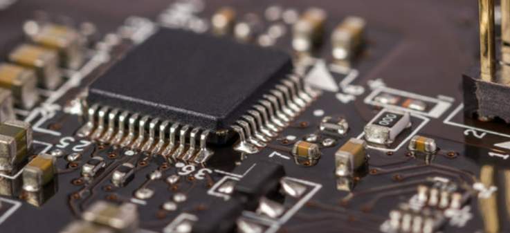
The increased cost caused by EMC on PCB board is usually caused by increasing the number of layers to enhance shielding effect and increasing ferrite bead and choke to inhibit high frequency harmonic devices. In addition, it is usually necessary to match the shielding structure on other organizations to make the entire system pass EMC requirements. The following are just a few tips for PCB board design to reduce the electromagnetic radiation effects generated by circuits.
When possible, use devices with slow signal slope (slew rate) to reduce slew components.
Ensure that the high-frequency components are not placed too close to external connectors.
Pay attention to the impedance matching, routing layer and return current path of high speed signal to reduce the reflection and radiation of high frequency.
Sufficient and appropriate de-coupling capacitors are placed in the power pins of each device to mitigate noise at the power layer and on the ground. Pay special attention to whether the frequency response and temperature characteristics of the capacitor meet the design requirements.
The ground near the external connector can be properly separated from the ground and connected to the chassis ground.
The ground guard/shunt traces can be properly applied to some particularly high speed signals. However, pay attention to the influence of guard/shunt traces on the characteristic impedance of the line.
The power layer is 20H smaller than the inside of the formation. H is the distance between the power layer and the formation.
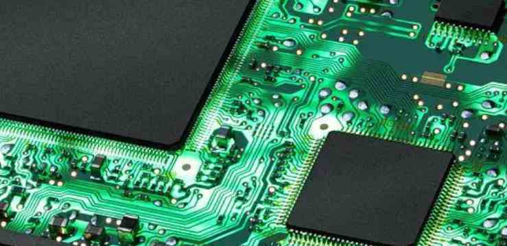
1. When there are multiple number/mode function blocks in a PCB board, the conventional practice is to separate the number/mode. Why?
The reason for separating digital/mode ground is that digital circuit will produce noise in the power supply and ground when switching between high and low potential, and the noise size is related to the signal speed and current size. If the ground plane is not divided and the noise generated by the circuit in the digital region is large and the circuit in the analog region is very close, the analog signal will still be disturbed by the ground noise even if the digital-analog signal does not cross. That is to say, the digital-to-analog undivided way can only be used when the analog circuit area is far away from the digital circuit area that generates large noise.
2, another method is to ensure that the number/mode layout is separate, and the number/mode signal lines do not cross each other, the whole PCB board is not divided, the number/mode ground are connected to the ground plane. Why?

The requirement that digital/analog signals should not cross is that the return current path of digital signals with a higher speed will flow back to the source of digital signals along the ground near the lower part of the line as far as possible. If the digital/analog signals cross, the noise generated by the return current will appear in the analog circuit area.
3. How to consider impedance matching when designing schematic diagram of high-speed PCB design?
Impedance matching is one of the key factors in designing high speed PCB circuits. The impedance value has an absolute relationship with the wiring mode. For example, the distance between the surface layer (microstrip) or the inner layer (stripline/double stripline), the distance from the reference layer (power layer or ground), the width of the wire, PCB material and so on will affect the characteristic impedance value of the wire. That is to say, the impedance value can be determined after wiring. General simulation software will not be able to take into account some impedance discontinuity wiring due to the error of the line model or the mathematical algorithm used. At this time, only some terminators(terminators), such as series resistors, can be reserved on the schematic diagram to mitigate the effect of impedance discontinuity. The real fundamental solution to the problem is to avoid impedance discontinuity when wiring as much as possible.
4. Where can I provide a more accurate IBIS model library?
The accuracy of IBIS model directly affects the result of simulation. Basically, IBIS can be regarded as the electrical characteristic data of the actual chip I/O buffer equivalent circuit, which can be converted by SPICE model (measurement can also be used, but there are more details). SPICE data is absolutely related to chip manufacturing, so different chip manufacturers provide the same device. The SPICE data is different, and the data in the converted IBIS model will also be different. In other words, if Manufacturer A's device is used, only they will be able to provide accurate model data of their device, because no one else will know better than they what process their device is made from. If the IBIS provided by the manufacturer is not accurate, the only solution is to constantly ask the manufacturer to improve.
How to choose PCB surface treatment process?
2023-03-30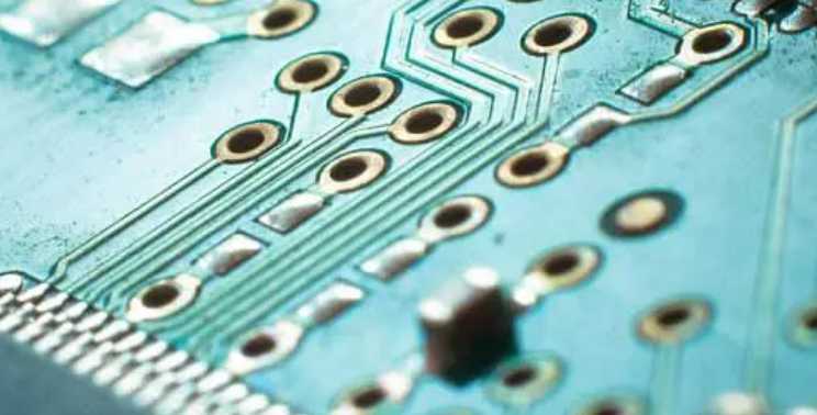


Достаточно загрузить файлы Gerber, BOM и проектные документы, и команда KINGFORD предоставит полное предложение в течение 24 часов.