
Контрактное производство электроники под ключ в Китае
Шэньчжэнь, район Баоань, улица Фуюн, улица Фуцяо, район 3, промышленный парк Лонгхуй 6


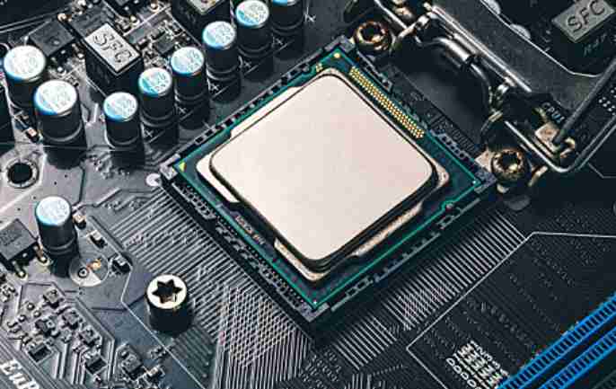
Not all PCB board processing manufacturers can guarantee every design and processing without accidents, sometimes due to various circumstances will lead to PCB board problems, need to rework and repair. However, pcb board processing in the rework repair is not random, but there are certain principles. What are the principles? Let's take a look.

1. The basis for rework and repair during pcb board processing is that the designer and production personnel, after production in accordance with the pcb board design document, find that it is not in harmony with the reality, so it must be repaired. The rework and repair also have unified process rules, which can not be messed with randomly.
2, each time in the pcb board processing process, the welding spot allowed rework times are limited. Some novice pcb board processing personnel think that as long as the mistake on the rework repair on the line, no big deal. But in fact, according to the production principle, there is a certain number of welding spot rework limits, basically no more than three times, otherwise it will cause damage to the welding site, and then lead to the pcb board performance is affected. Therefore, once three times of rework occurs, basically this pcb board will not be used again.
3, for pcb board processing and repair will meet the disassembly of components, in principle, the disassembled components can not be used again. Even if it is to be used, it must be screened to determine that it meets the requirements before it can be used again. Here, Xiaobian gives you a small hint, some small workshops or unruly and unprofessional pcb board processing small manufacturers in order to save costs, will rework and repair disassembled components secondary use, such a practice is not correct, although the cost is saved, but in fact the performance is affected. Therefore, some small workshop type pcb board processing plants are cheap, the reason is this.
4, pcb board processing, the number of welding on the pad is also specified. According to the designer of the regular pcb board processing manufacturer, each printed pad is basically a one-time operation, and only one component is allowed to be replaced, because the thickness of a qualified solder joint will increase after remelting, resulting in a brittle solder joint and a decline in strength. In the case of vibration, it is very easy to bring safety risks to electronic products. Therefore, regular pcb board processing manufacturers will not often secondary soldering.
5. When remelting, the required temperature is higher, which will have a certain impact on pcb board, especially the IMC needs to be removed, so a certain high temperature must be maintained. The high temperature will lead to fracture or deformation of the copper plating layer, and eventually lead to the release of the pad. In addition, in the case of lead-free, high temperature will also make the whole pad pull up, and finally be heated stratification, warping or separation phenomenon.
The above is the principle of rework and repair in pcb board processing. Although troublesome, it can ensure the quality of production and processing, and let customers have no worries. Therefore, pcb board processing manufacturers must strictly comply with, only in this way, to ensure their own corporate image, to attract more customers to cooperate.
How to determine the number of PCB connecting boards?
Generally speaking, after the design engineer has determined the printed circuit board's appearance, the panelization of the circuit board should proceed immediately. The purpose of connecting plates is nothing more than the following:
1. Increase the output of production line.
2, reduce the loss of plate.
The most common connected board usually combines more than two pieces of the same circuit board into a large circuit board, such as 2 in 1 (two-in-one), 3 in 1 (three-in-one), 4 in 1 (four-in-one), etc. There was also a case where boards of different shapes were made into a large board, but this was rare because it was difficult for the Planner to arrange production with just the right number of different boards.
There are also examples of making the same board into "Yin Yang board". "Yang Yang board" mostly means top and bottom surface configuration, which is usually used on circuit boards with fewer parts, such as mobile phone board, because it can make full use of SMT's long line hitting function to increase efficiency, but the disadvantage is that the use is limited. And may cause parts heat uneven phenomenon, for example, some circuit boards will put the heavy parts concentrated design of a side, and then this side will be as a second hit to avoid heavy parts repeated reflow fall, of course, this board is more difficult to use [Yin and Yang board] design.
Some boards may have more heat-absorbing parts (such as a large area of ATM card slot), and are not suitable for the design of [Yin and Yang board]. Of course, there are also flexible [Yin and Yang plate] typing method can overcome this problem, but not to discuss.
Basically, in the design of how much even board, should consider the following factors, in fact, no matter how to produce or design, ultimately can not be separated from the consideration of money, so should all the factors into the amount to make the final measurement standard to choose a suitable plate method.


Достаточно загрузить файлы Gerber, BOM и проектные документы, и команда KINGFORD предоставит полное предложение в течение 24 часов.