
Контрактное производство электроники под ключ в Китае
Шэньчжэнь, район Баоань, улица Фуюн, улица Фуцяо, район 3, промышленный парк Лонгхуй 6

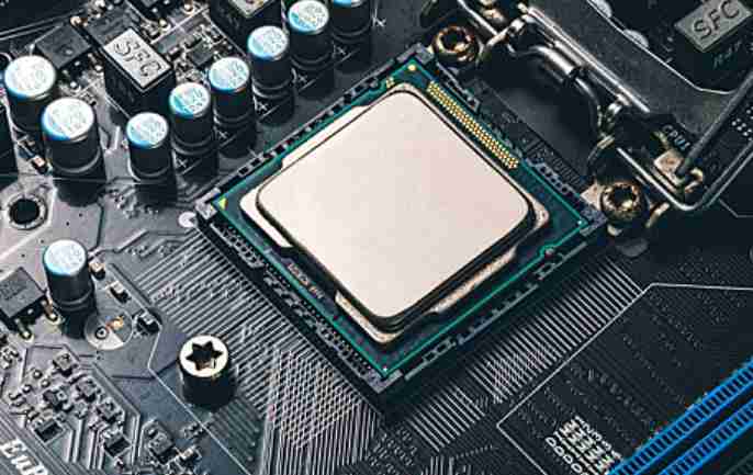
There are four main electroplating methods in the circuit board: finger plating, through hole plating, coil continuous selective plating, brush plating.
Here is a brief introduction:
1. Finger row electroplating equipment
In plating, rare metals often need to be plated on plate edge connectors, plate edge protruding contacts or gold fingers to provide lower contact resistance and higher wear resistance. This technique is called finger plating or protruding part plating.
In electroplating, gold plating is often plated on the inner layer of nickel plate edge connector protruding contact, gold finger or plate edge protruding part of manual or automatic plating technology, at present, the gold plating on the contact plug or gold finger has been replaced by lead plating, plating button.
2. Through hole electroplating
In through-hole electroplating, there are several ways to build a suitable coating on the hole wall of the substrate drilled, which is called hole wall activation in industrial applications. The commercial production process of printed circuit requires several intermediate storage tanks, each of which has its own control and maintenance requirements.
Through hole electroplating is a necessary follow-up to the drilling process. As the bit drills through the copper foil and its underlying substrate, the heat generated melts the insulating synthetic resin that makes up most of the substrate substrate. The melted resin and other drilling debris are deposited around the holes and coated on the newly exposed hole walls of the copper foil.
In fact, this is harmful to the subsequent plating surface. The melted resin will also leave a layer of thermal shaft on the hole wall of the substrate. It shows poor adhesion to most activators, which requires the development of another technology similar to the chemical action of stain removal and erosion: ink!

The ink is used to form a highly adhesive, highly conductive film on the inner wall of each through-hole, so that it does not have to use multiple chemical processing processes, only one application step, followed by thermal curing, can form a continuous film on the inside of all the hole walls, it does not need further processing can be directly plated. The ink is a resin-based material that is highly adhesive and can be easily attached to most hot polished perforated walls, eliminating the need for erosion.
3, rolling wheel continuous selective plating
Pins and pins of electronic components, such as connectors, integrated circuits, transistors and Flexible printed circuits, are selected plating for good contact resistance and corrosion resistance.
This plating method can use manual plating production line, can also use automatic plating equipment, separate selection of each needle plating is very expensive, so must be used in batch welding, usually in plating production will be rolled into the required thickness of the metal foil at both ends of the punching, using chemical or mechanical methods for cleaning, and then selective use like nickel, gold, silver, rhodium, button Or tin nickel alloy, copper nickel alloy, nickel lead alloy for continuous plating.
4, brush plating
The final method is called "brush plating" : it is an electrodeposition technique in which not all parts of the plating process are immersed in the electrolyte. In this electroplating technique, only a limited area is plated and the rest is not affected at all.
Usually, rare metals are plated on selected parts of the printed circuit board, such as areas such as board edge connectors. Brush plating is used more often in electronics assembly shops to repair discarded circuit boards. A special anode (chemically inactive anode, such as graphite) is wrapped in an absorbent material (cotton swabbed) and used to carry the plating solution to the site where the plating is to be performed.
What are the reasons for short circuit of PCB board after wave soldering
Wave soldering if improper operation will cause a lot of PCB welding points short circuit tin phenomenon. PCB welding point short circuit and tin is also the most bad welding manufacturers in wave soldering, it is caused by a variety of reasons. The following and you analyze the PCB board after wave soldering short circuit tin reasons.
1. The tin liquid has not reached the normal working temperature, and there is a "tin wire" bridge between solder joints.
2. The direction of the substrate is not compatible with the tin wave, and the direction of eating tin is changed.
3, poor line design: the line or contact is too close to each other (there should be more than 0.6mm spacing); If it is a aligned solder joint or IC, it should be considered to steal the solder pad, or use text white paint to separate it. At this time, the thickness of the white paint should be more than 2 times the thickness of the welding pad (golden channel).
4. The polluted tin or the accumulation of too much oxide is brought by the PUMP to cause short circuit. The tin furnace should be cleaned or all the solder in the tin tank should be updated.
5, even tin may be preheating temperature is not enough to lead to the element method to reach the temperature, welding process due to the element heat absorption, resulting in poor drag tin, and the formation of tin; It could also be that the temperature of the tin furnace is too low, or the soldering speed is too fast.
Through the above five points of analysis, we should be able to find the cause of short circuit tinning of PCB board after wave soldering. If we still cannot find the cause through the above five points of investigation, it is probably the wave soldering problem. For example, the actual temperature of the display and wave soldering is different.


Достаточно загрузить файлы Gerber, BOM и проектные документы, и команда KINGFORD предоставит полное предложение в течение 24 часов.