
Контрактное производство электроники под ключ в Китае
Шэньчжэнь, район Баоань, улица Фуюн, улица Фуцяо, район 3, промышленный парк Лонгхуй 6

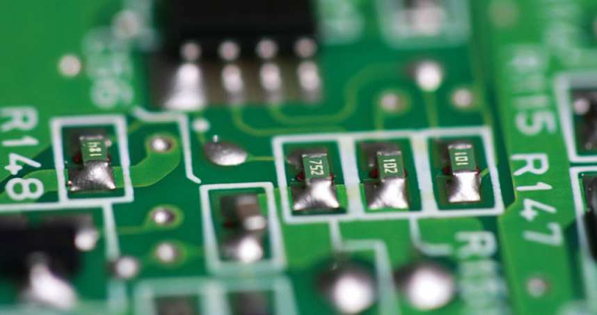
The inspection after PCB welding is very important for enterprises and customers, especially many enterprises have strict requirements on electronic products, if not checked, it is easy to appear performance failures, affect product sales, but also affect the corporate image and reputation. Then, how to check the quality of PCB after welding?
1, PCB triangulation method
What is triangulation? The method used to check the three-dimensional shape. Triangulation methods have been developed and devices designed to detect the shape of the cross-section have been developed, however, because the triangulation method is incident from different light in different directions, the results of the observation will be different. In essence, the object is tested through the principle of light diffusivity. This method is the most appropriate and the most effective. As for the welding surface close to mirror condition, this way is not suitable, it is difficult to meet the production demand.
2, light reflection distribution measurement method

This method mainly uses welding parts to detect decoration, inward incident light from the tilt direction, sets TV camera above, and then inspects it. The most important part of this operation method is how to know the surface Angle of PCB solder, especially how to know the illumination information, etc., it is necessary to capture the Angle information through various lighting colors. On the contrary, if it is illuminated from above, the measured Angle is the reflected light distribution. Check the tilted surface of the solder.
3, change the Angle of the camera inspection
How to detect PCB after welding? Using this method to detect PCB quality after welding, it is necessary to have a device with changing Angle. This device usually has at least 5 cameras, multiple LED lighting equipment, will use multiple images, using visual conditions for inspection, relatively high reliability.
4. Focus detection and utilization method
For some high-density circuit boards, it is difficult to detect the final results by the above three methods after PCB welding, so the fourth method, focus detection and utilization method, is needed. This method is divided into several, such as multi-segment focus method, which can directly detect the height of the solder surface, to achieve high precision detection method, at the same time set 10 focus surface detector, you can obtain the focus surface by seeking the maximum output, to detect the position of the solder surface. If it is detected by shining a micro laser beam on the object, as long as 10 specific pinholes are staggered in the Z direction, the 0.3mm pitch lead device can be detected successfully.
The above four methods are some detection methods used by PCBA processing manufacturers for external inspection of PCB boards.
With the above foundation, we know that it is not difficult to make two double panels "stick" together! For example, we make a typical four-layer board (divided into 1~4 layers in order, among which 1/4 is the outer layer, signal layer, 2/3 is the inner layer, grounding and power layer). First, we make 1/2 and 3/4 (the same substrate) respectively, and then glue the two substrates together. But this binder is not an ordinary glue, but a softened resin material, it is first insulated, second very thin, and good adhesion to the substrate. We call it pp material, its specification is the thickness and the amount of glue (resin). Of course, the general four layer board and six layer board we can not see, because the thickness of the six layer board is relatively thin, even if you want to use two layers of pp three double-sided substrate, it is not necessarily more than a layer of pp two double-sided substrate of the four layer board can increase how much thickness - the thickness of the board has a certain specification, otherwise it can not be inserted into a variety of card slot. At this point, the reader will ask, isn't the signal between the layers supposed to be switched on? Now pp is an insulating material, how to realize the interconnection between layers? Don't worry, we need to drill holes before we can bond the multilayer! Drilling holes can be the corresponding positions of the circuit board up and down copper wire, and then let the hole wall with copper, then is not equivalent to the wire will be connected in series?
It's called the plating hole, or pt hole for short. These holes need to be drilled by a drilling machine. Modern drilling machines can drill very small holes and very shallow holes. There are hundreds of holes of different sizes and depths on a single motherboard. plated-through-hole technology (pth) is then applied to the hole after drilling the hole.
The holes are drilled, the inner and outer layers are connected, and the multilayer panels are glued. Is that done? Our answer is no, because the motherboard production needs a lot of welding, if direct welding, will produce two serious consequences: one, the surface of the copper wire oxidation, welding; Two, the phenomenon of lap welding is serious - because the spacing between the lines is too small! So we have to cover the whole pcb substrate with a layer of armor -- this is the solder resistance paint, also known as solder resistance, which has no affinity for liquid solder, and will change and harden under specific spectrum of light irradiation. This property is similar to dry film. The color of the board we see is actually the color of solder resistance paint, if the solder resistance paint is green, So the card is green.
Finally, don't forget screen printing, gold finger gilding (for the graphics card or pci card) and quality control, test whether there is a short circuit or open circuit pcb condition, you can use optical or electronic test. The optical method uses scanning to find defects in each layer, and the electronic test usually uses a flying probe to check all connections. Electronic tests are more accurate at finding short or open circuits, but optical tests can more easily detect incorrect gaps between conductors.


Достаточно загрузить файлы Gerber, BOM и проектные документы, и команда KINGFORD предоставит полное предложение в течение 24 часов.