
Контрактное производство электроники под ключ в Китае
Шэньчжэнь, район Баоань, улица Фуюн, улица Фуцяо, район 3, промышленный парк Лонгхуй 6

1. Printed circuit board (printed circuit board, PCB)
PCB is short for Printed Circuit Board (namely Printed Circuit Board). Also known as printed circuit board, printed circuit board, because it is produced by electronic printing technology, it is called "printed" circuit board. A printed circuit board is a substrate for assembling electronic parts. It is a printed board that forms point-to-point connections and printed components according to a predetermined design on a general substrate. The main function of the product is to make a variety of electronic components form a predetermined circuit connection, play the role of relay transmission, is the key electronic interconnection of electronic products, known as the "mother of electronic products". PCBS are used as the substrate and key interconnect for electronic parts, and are required for any electronic equipment or product.
Two, PCB manufacturing principle
We open the keyboard of a general-purpose computer and see a soft film (flexible insulating material) printed with a silver-white (silver paste) conductive pattern and a health pattern. Because of the general screen leakage method to get this pattern, so we call this printed circuit board flexible silver printed circuit board. And we go to the computer city to see a variety of computer host boards, graphics cards, network cards, modems, sound cards and household appliances on the printed circuit board is different. The substrate used is made of paper base (usually used for single side) or glass cloth base (usually used for double side and multilayer), prepreg phenolic or epoxy resin, one or both surface layers glued to a copper sheet and then laminate and cure. This kind of circuit board covered with copper sheet plate, we call it rigid plate. To make printed circuit board, we call it rigid printed circuit board. Single-side printed circuit board we call single-side printed circuit board, double-side printed circuit board, and then through the metallization of the hole for double-side interconnection, we call it a double panel. If a double-sided for the inner layer, two single-sided for the outer layer or two double-sided for the inner layer, two single-sided for the outer layer of the printed circuit board, through the positioning system and insulating binder material alternating together and conductive graphics in accordance with the design requirements of the interconnected printed circuit board will become a four-layer, six-layer printed circuit board, also known as the multi-layer printed circuit board. There are now over 100 layers of functional printed circuit boards.

3. PCB production process
PCB production process is more complex, it involves a wide range of processes, from simple mechanical processing to complex mechanical processing, there are ordinary chemical reactions and photochemical electrochemical thermal chemistry and other processes, computer aided design CAM and other aspects of knowledge. In addition, there are many technological problems in the production process and new problems will be encountered from time to time. Some of the problems will disappear without finding out the causes. Because the production process is a discontinuous assembly line, any problem at any link will result in the whole line being stopped or a large number of scrapped consequences. Process engineers can be stressful, so many engineers leave the industry to work in sales and technical services for PCB equipment or materials companies.
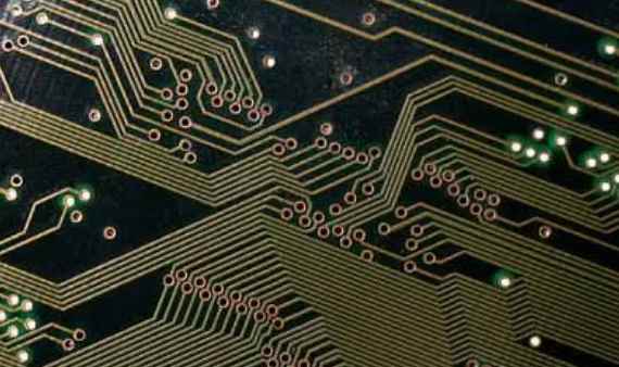
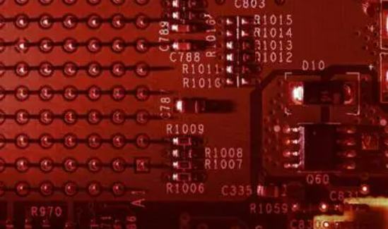
The substrate of the board itself is made of an insulating, non-bendable material. The small wire material that can be seen on the surface is copper foil. Originally, copper foil is covered on the whole board, but in the manufacturing process, the middle part is etched away, and the remaining part becomes a network of small lines. These circuits are called conductor patterns, or wiring, and are used to provide circuit connections for parts on the PCB.
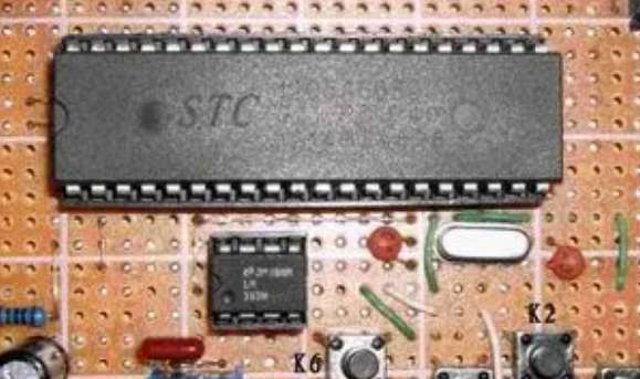
To secure the parts to the PCB, we solder their pins directly to the wiring. On the most basic PCB(single panel), the parts are concentrated on one side and the wires on the other. In this way, we need to make holes in the board so that the connector can go through the board to the other side, so the connector of the part is welded to the other side. Because of this, the front and back of the PCB are respectively called Component Side and Solder Side.
If there are parts on the PCB that can be removed or put back on after the PCB is made, the Socket is used when the part is installed. As the socket is directly welded on the board, the parts can be arbitrarily disassembled.
To connect two PCBS to each other, we usually use the edge connector known as the "golden finger". The finger contains a number of exposed copper pads that are actually part of the PCB wiring. Usually to connect, we insert the gold finger on one PCB into the appropriate Slot on the other PCB (generally called an expansion Slot). In computers, interface cards such as video cards, sound cards, and the like are connected to the main board by the goldfinger.


Достаточно загрузить файлы Gerber, BOM и проектные документы, и команда KINGFORD предоставит полное предложение в течение 24 часов.