
Контрактное производство электроники под ключ в Китае
Шэньчжэнь, район Баоань, улица Фуюн, улица Фуцяо, район 3, промышленный парк Лонгхуй 6

kingford is a professional PCB design company engaged in electronic products layout layout design, mainly undertake multi-layer, high density PCB design and circuit board design proofing business. Next, from the welding point of view, talk about the design of PCB need to pay attention to what points.
1. Factors affecting PCB welding quality
From PCB design to the completion of all components welding, to become a high quality circuit board, PCB engineers, welding technology, welding workers and many other links to control.
There are mainly the following influencing factors: PCB diagram, the quality of the circuit board, the quality of the device, the oxidation degree of the device pin, the quality of the solder paste, the printing quality of the solder paste, the accuracy of the program of the placement machine, the mounting quality of the reflow furnace temperature curve and so on.
The welding plant itself is impassable link is PCB drawing.
Circuit designers rarely weld circuit boards, unable to obtain rich welding experience, and welding factory workers do not understand the drawing board, just complete the production task, have no mind, more have no ability to analyze the causes of bad welding.
These two aspects of the talent play their own roles, difficult to combine organically.
2. Suggestions when drawing PCB
Here are some tips to avoid the various bad drawings that can affect the quality of welding.
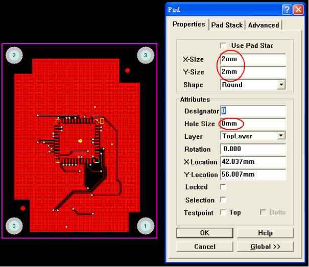
1. About the positioning hole
Four holes (minimum aperture 2.5mm) should be left at the four corners of the PCB board for positioning the circuit board when printing solder paste. I want the center of the X or Y axis to be on the same axis
2. About the MARK point
The PCB board should be marked with Mark points for placement machine positioning.
Specific position: In the diagonal of the plate, it can be a round or square pad, do not mix with the pad of other devices. If there are devices on both sides, both sides should be marked
You can also consider adding MARK points to your collage.
3. When designing PCB, please pay attention to the following points:
The shape of point a and Mark is as follows: symmetrical up and down or symmetrical left and right.
The dimensions of b and A are 2.0mm.
c. There should be no shape and color changes that may cause misidentification within 2.0mm from the outer edge of Mark point. (pad and paste)
d. The color of Mark point should be different from the color of PCB around it.
e. In order to ensure the accuracy of identification, the surface of the Mark point is electroplated with copper or tin to prevent reflection. The shape is only marked by lines, light points can not be recognized.

4. Leave 5mm edge
When drawing PCB, no less than 3mm edge should be left in the long side direction for the placement machine to transport the circuit board, and the placement machine cannot mount the device within this range. Do not place patch devices within this range.
For the circuit board of double-sided decoration, consider the secondary reflow welding, the device is rubbed off, the pad is rubbed off and so on.
It is suggested that on the side with fewer chips, the long side should be within 5mm from the side. If it is true that the area of the circuit board is limited, the process edge can be added on the long side.
5, do not directly in the pad over the hole
When the pad is perforated, solder paste will flow into the hole in reflow welding, causing the solder shortage of the device pad and causing virtual welding
6. Polarity labeling of diode and tantalum capacitor
Polarity marking of diode and tantalum capacitor is in line with industry regulations, so as not to weld the wrong direction by experience
7. Screen printing and signage
Please hide the device model. Especially the circuit board with high device density. Otherwise, dazzle the effect of finding the welding position.
And don't just label the model, not the label. As shown in the figure below, it is impossible to program the chip machine.
About screen printing and signage
The size of the silk screen characters should not be too small, and the characters should be staggered over the holes to avoid misreading.
8. IC welding pad should be extended
For IC packaged with SOP, PLCC, QFP, etc., the length of pad on PCB = length of IC foot ×1.5 is appropriate. When manual soldering iron is used, chip pins and PCB pad and tin are fused into one
The IC pad should be extended
9, about the width of IC pad
SOP, PLCC, QFP package IC, drawing PCB should pay attention to the width of pad, pad a width on PCB =IC foot width (Nom in datasheet. Value), it is not recommended to widen, to ensure that the spacing b between two pads has enough width to avoid continuous welding.
10. Do not rotate the device at any Angle
Since the SMT machine cannot rotate at any Angle, it can only rotate 90℃, 180℃, 270℃ and 360℃.
After attaching the device pin and the welding pad on the circuit board, the Angle will be staggered by 1℃, thus affecting the welding quality.
Do not rotate the device at any Angle
11. Problems that should be paid attention to when the adjacent pin is short connected
12. About the middle pad under the chip
For chips with belly, it is recommended to narrow the middle pad so as to increase the distance between it and the surrounding pad and reduce the chance of short circuit.
It's about the middle pad under the chip
13. Two devices of higher thickness should not be closely lined up
The cloth plate will cause the SMT machine to encounter the previous attached device when attaching the second device, and the machine will detect the danger, resulting in automatic power failure.
Do not close together two devices of higher thickness
14. About the BGA
Because the BGA package is special, its pad is under the chip, and the welding effect can not be seen outside.
To facilitate repair, it is recommended to drill two positioning holes with Hole Size of 30mil on the PCB board to locate the steel mesh during repair.
Warm tip: The size of the positioning hole should not be too large or too small. It is appropriate to make the needle not fall off after insertion, not shake, and a little tight when insertion, otherwise the positioning is inaccurate.
About BGA
15. About PCB board color
Red is not recommended. The red circuit board is white under the red light source of the camera of the patch machine, which cannot be programmed and is not convenient for the welding of the patch machine.
16, about the small device under the big device
Some people like to line up the smaller devices under the larger ones. For example, the digital tube has a resistor under it.
This layout will cause difficulties to repair, repair must be removed first, and may cause damage to the digital tube. It is recommended to drain the resistance under the digital tube to the Bottom surface.
17, about the impact of copper coating and welding plate connected to molten tin
Because the copper coating will absorb a lot of heat, resulting in the solder is difficult to fully melt, resulting in the formation of virtual welding.
The device pad is directly connected with the copper coating; Although the 50Pins connector is not directly connected with the copper coating, since the middle two layers of the four layers of the board are covered with copper in a large area, Fig.A and Fig.B will not be able to melt the solder paste fully due to the heat absorbed by the copper coating.
The body of 50Pins connector is a high temperature resistant plastic. If the temperature is set high, the connector will melt or deform. If the temperature is set low, the copper coating will absorb a lot of heat and cause the solder paste to not melt fully. Therefore, it is recommended that the pad be isolated from large area copper coating.
18. Suggestions on the board and adding process
summarize
Nowadays, more and more engineers can use software to draw, design and route PCB board. After the design is completed, the welding efficiency can be improved. The author believes that the above factors should be paid attention to.


Достаточно загрузить файлы Gerber, BOM и проектные документы, и команда KINGFORD предоставит полное предложение в течение 24 часов.