
Контрактное производство электроники под ключ в Китае
Шэньчжэнь, район Баоань, улица Фуюн, улица Фуцяо, район 3, промышленный парк Лонгхуй 6

Before producing printed circuit board, the following steps are generally followed
1. Preliminary preparation
The preliminary preparation contains the preparatory component library and schematic diagram. Before PCB planning, the schematic SCH component library and PCB component packaging library should be prepared first.
The PCB component package library is best established by the engineer according to the standard scale material of the selected equipment. In principle, first set up PC component packaging library, and then set up schematic SCH component library.
PCB component packaging library has high requirements, which directly affects the PCB device; Schematic SCH component library requirements are relatively loose, but pay attention to the definition of pin characteristics and the corresponding relationship with the PCB component packaging library.
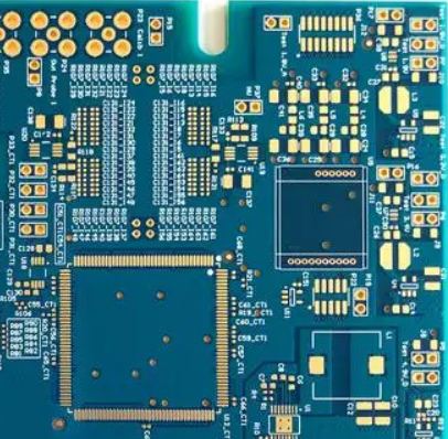
2. PCB structure planning
According to the accepted size of the circuit board and various mechanical positioning, the PCB board frame is drawn in the PCB planning environment, and the required connectors, keys/switches, screw holes, mounting holes, etc. are placed according to the positioning requirements.
Wiring and non-wiring areas are fully considered and recognized (e.g., how much of the screw hole is around the non-wiring area).
3. PCB layout planning
Layout planning is to place devices in PCB board frames according to the planning requirements. Generate the network table (Design→Create Netlist) in the schematic tool, and then Import the network table (Design→ import Netlist) in the PCB software. After the successful import of the network table will exist in the software background, through the Placement operation can be all equipment out, there is a flying line between the pins connection, then you can carry out the layout planning of the equipment.
PCB layout planning is the first important process in the whole PCB planning process. The more chaotic the PCB board is, the better the layout will directly affect the completion of the wiring.
Layout planning depends on the circuit foundation of circuit board planner and the richness of planning experience, the circuit board planner belongs to a higher level of requirements. Junior circuit board planner experience is relatively shallow, suitable for small module layout planning or the whole board of low difficulty PCB layout planning tasks.
4. PCB routing planning
PCB routing planning is the most workload process in the whole PCB planning, which directly affects the function of PCB board.
In the planning process of PCB, wiring generally has three levels:
First is the cloth, which is the most basic entry requirements of PCB planning;
The second is the satisfaction of electrical function, which is a measure of whether a PCB board qualified standard, after the line layout, carefully adjust the wiring, so that it can reach the best electrical function;
Again is neat and beautiful, disorderly wiring, even if the electrical function clearance will also bring great inconvenience to the later board optimization and test and maintenance, wiring requirements neat and uniform, can not have no rules.
5. Wiring optimization and silk-screen placement
"PCB planning is not the best, only better", "PCB planning is a defective art", this is mainly because PCB planning needs to complete all aspects of hardware planning, and individual requirements may be conflicting, can not have both.
For example, a PCB planning project needs to be planned into 6 layers after evaluation by the circuit board planner, but the product hardware needs to be planned into 4 layers due to cost consideration, so the signal shielding layer can only be sacrificed, and then the signal crosstalk between adjacent wiring layers will be added, and the signal quality will be reduced.
General planning experience is: the time of optimization wiring is twice the time of initial wiring. After optimizing the PCB routing, you need to perform post-processing. The first step is to process the silkscreen logo on the PCB board. During the planning, you need to mirror the characters on the bottom layer to avoid confusion with the top layer silkscreen.
6. Check the network DRC and structure
Quality control is an important part of PCB planning process. General quality control means include: planning self-check, planning mutual check, expert evaluation meeting, special inspection, etc.
Schematic diagram and structure element diagram are the most basic planning requirements. Network DRC viewing and structure viewing are separated from the two input conditions of PCB planning satisfaction: schematic diagram netlist and structure element diagram.
Generally, circuit board planners have their own accumulated planning quality Checklist, in which some items are based on company or department specifications and some are based on their own experiences. Special view includes planning Valor view and DFM view. These two parts attach importance to the back-end processing light drawing file of PCB planning output.
7, PCB board
Before the formal processing of PCB board, the circuit board planner needs to communicate with the PE of PCB plate supplier factory to answer the manufacturer's acknowledgement on PCB circuit board processing.
This includes but is not limited to: PCB board type selection, line width and line distance adjustment, impedance control adjustment, PCB laminated thickness adjustment, surface treatment processing technology, aperture service control and delivery standards.
PCB design skills of switching power supply
2023-02-16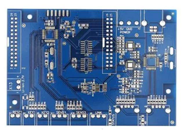


Достаточно загрузить файлы Gerber, BOM и проектные документы, и команда KINGFORD предоставит полное предложение в течение 24 часов.