
Контрактное производство электроники под ключ в Китае
Шэньчжэнь, район Баоань, улица Фуюн, улица Фуцяо, район 3, промышленный парк Лонгхуй 6

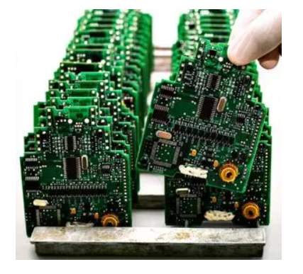
1.PCB is divided into single panel, double panel, multi-layer board, this classification is based on the number of layers, when the circuit becomes complex, PCB board wiring density increases, the same area of pcb a layer can not accommodate too much electrical route, so to pcb boardprocessing, plus two layers, three layers or even more layers, pcb board between layer and layer with conductive hole connection to achieve the purpose of conduction, is the whole pcb circuit board energized normal operation.
We see that pcb has several signal layers, called copper for short. However, the pcb we see is not a whole piece of copper skin, but covered with lines. These lines are etched with chemical methods to remove the excess part of the original layer of copper skin, leaving only the lines we want to SMT processing.
Because pcb circuit board to achieve a customer's required performance, it is necessary to expand the number of pcb layers to more than two layers, so many Shenzhen pcb manufacturers out of the multi-layer circuit board of the double panel. The more layers you have, the more complicated it gets. As a result of processing two or more layers of pcb board together, stacked on each other, the pcb board is set up to connect with each other. Production process is simple: open material - the inner line - lining etching - brown is changed, pressure plate, drilling - PTH/plate - the outer graphics - electroless nickel gold or tin - outer etching, QC, ET - gong plate - QA - shipments.
Multilayer board is generally put into use in professional electronic equipment, such as military, automobile, especially in the case of pcb overload, can only use multi-substrate to increase heat dissipation space and reduce weight.
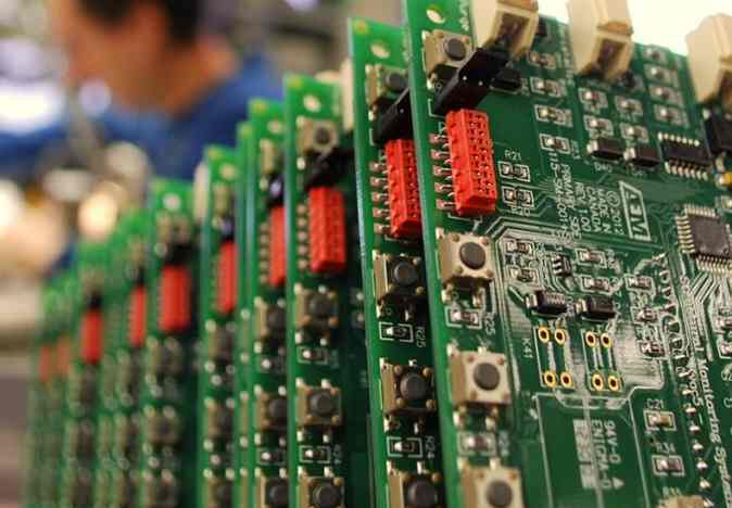
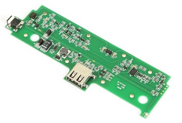
pcb board layer is divided into welding resistance layer and welding aid layer, as well as signal layer, SMD patch layer, no wiring layer, drilling layer. Welding layer is SMT patch processing to be used, is used to open the steel mesh with tin leakage. Most PCBS we see are green oil, because green oil is allowed for welding, and green oil should be applied to all areas without welding layer.

2. The use and storage of solder paste is the secret of SMT patch processing
There are many brands and types of solder paste in SMT patch processing. How to buy high quality solder paste is decided by the accumulated experience of SMT patch processing and professional purchasing personnel.
Solder paste is a denaturating fluid. The printing performance of solder paste in smt processing and the quality of solder paste graphics have great relationship with the viscosity and thixotropy of solder paste. Because the solder paste is mostly carried out in the air in the printing process at present, the temperature of the environment will also affect the quality of the solder paste. If the humidity is too high, the water vapor will mix with the solder paste. The serious consequence is that the solder ball will be oxidized and spattered during reflow welding in the smt patch, which is very dangerous and harmful to the product. The humidity is too small, easy to cause solvent volatilization in the solder paste and viscosity reduction, resulting in filling and film removal. Therefore, the storage environment of solder paste should be controlled, and the relative humidity is recommended to be controlled at (45%-70%) RH. The change of ambient temperature will also cause viscosity fluctuation, so the best effect is to control the ambient temperature at 23 degrees. There is another point that needs to be noted in SMT patches: the solder paste printing environment should be kept clean and sanitary. The dust in the air may cause pores in the printing. Therefore, the solder paste should be stored in a clean and sanitary, dust-free and corrosive gas free workshop.
Recommended storage method of solder paste:
1, if in the process of shipment, about 4 days, the temperature environment is controlled at < 10 ℃
2, shelf life (refrigerated), about 3~6 months, its temperature environment in the refrigerator 0-5℃
3. The solder paste is removed from the refrigerator at a stable time within 8 hours, the humidity is 30%-60%RH, and the ambient temperature is 15%-25%℃
In the use of solder paste is to pay attention to the following requirements:
1. After the arrival of the solder paste, the time and shelf life of the solder paste should be timely arrived, the model of the solder paste, and the number of each can of the solder paste should be written.
2. The solder paste should be stored in a sealed form in a constant temperature and humidity refrigerator, at a temperature of 2-10℃.
3. If SMT is to be applied, the solder paste should be taken out of the refrigerator at least 4 hours in advance, and the time, number, user and corresponding product should be written down after taking out, and the solder paste should reach the working room temperature before opening the cap. If opened before the temperature has not risen, it will lead to the solder paste easy to absorb gas, reflow welding will occur tin beads. (Note: do not directly put the solder paste next to the heat exchanger and air conditioning etc.)
4. After the tin paste is unsealed, it should be stirred for at least 5 minutes to make the ingredients of the tin paste even.
5. According to the number of devices in the smt patch, the format of the printed circuit board should be evenly printed. Generally, 200-300 grams should be added once, and a little can be added appropriately after printing.
6. When printing solder paste and SMT patch operation, it is required to hold the edge of pcb or wear gloves. To prevent contamination of pcb.
Some notes on the use of solder paste and storage method, hope to be helpful to readers


Достаточно загрузить файлы Gerber, BOM и проектные документы, и команда KINGFORD предоставит полное предложение в течение 24 часов.