
Контрактное производство электроники под ключ в Китае
Шэньчжэнь, район Баоань, улица Фуюн, улица Фуцяо, район 3, промышленный парк Лонгхуй 6

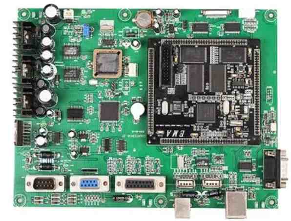
1. What should we pay attention to in SMT patch processing to ensure quality? The following details should be noted:
1. The Mark point is round or square, with a diameter of 1.0mm, depending on the equipment of SMT. The copper area around the Mark point should be larger than 2.0mm, and creases, dirt and copper exposure are not allowed at the Mark point;
2. The four corners of each large board must have a Mark point or two Mark points in the diagonal, Mark point from the edge needs to be greater than 5mm;
3. Each small board must have two Mark points;
4. According to the detailed equipment and effectiveness evaluation, FPC assembling board is not allowed to have "X" board;
5. When fixing the board, the crux area will be glued to the board with a wide adhesive paper, and then check the film. If the fixing board is not flat, it must be pressurized again and check the film again.
6. 0402 component pad spacing is 0.4mm; The spacing between 0603 and 0805 components is 0.6mm; The pad is best disposed into a square;
7. In order to prevent FPC board small area because of punching subsidence, from the bottom of the bias punching;
8. After the FPC board is made, it must be baked and vacuum packed; Before SMT goes on line, it is best to pre-bake;
9. The size of the panel should be within 200mmX150mm;
10. There shall be four positioning holes for SMT fixture at the edge of the assembly plate, the aperture of which is 2.0mm;
11. The minimum interval between the edge element of the plate and the edge of the plate is 10mm;
12. Board distribution try to spread each small board in the same direction;
13. The goldfinger area of each small plate (i.e., hot pressed end and weldable end) is pieced together to prevent goldfinger from eating tin in SMT production; From :www.PCBa-smt.cn
14. The minimum spacing between Chip components and pads is 0.5mm.

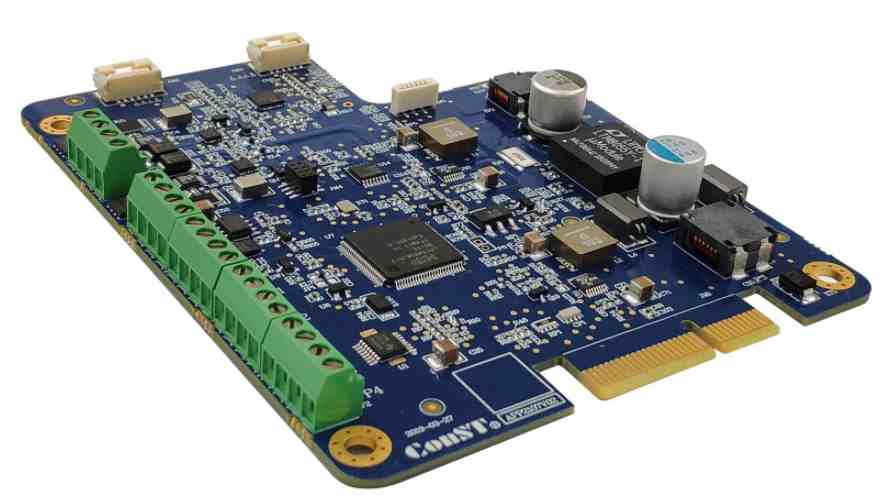
2. What special points should be paid attention to in SMT patch processing?
SMT patch is one of the basic components of electronic components, known as the outside assembly skills, divided into no pin or short lead, is through the process of reflow welding or dip welding to weld the circuit assembly skills, is also the most popular technology in the electronic assembly industry. Through the SMT technique to mount more smaller and lighter components, so that the circuit board to complete the detailed, miniaturization request, which is the SMT SMT processing skills request higher.
First, SMT patch processing solder paste necessary attention:
1, constant temperature: it is proposed that the storage temperature in the refrigerator is 5℃-10℃, do not be less than 0℃.
2, warehouse: must abide by the principles of the previous generation, do not form tin paste in the freezer storage time is too long.
3. Freezing: Take out the solder paste from the freezer and freeze it naturally for up to 4 hours. When freezing, you can not close the cap.
4, the situation: proposed workshop temperature of 25±2℃, relative humidity in 45%-65%RH conditions applied.
5. Applied old solder paste: the solder paste after opening the lid is recommended to be used up within 12 hours. If you need to keep it, please use clean empty bottle to fill it, and then seal it and put it back in the freezer to keep.
6. The amount of paste placed on the steel net: the amount of solder paste placed on the steel net for the first time should not exceed 1/2 of the height of the scraper when printing rotation. It is better to check frequently and add less frequently.
2. It is necessary to pay attention to SMT patch processing and printing work:
1. Scraper: steel scraper is the best material for scraper, which is conducive to forming and removing film of tin paste printed on PAD.
Scraper Angle: manual printing 45-60 degrees; Mechanical printing is 60 degrees.
Printing rate: manual 30-45mm/min; Printing press 40mm-80mm/min.
Printing conditions: Temperature at 23±3℃, relative humidity 45%-65%RH.
2, steel mesh: steel mesh hole according to the product of the request to choose the thickness of steel mesh and hole shape, proportion.
QFP\CHIP: Laser hole is required for CHIP with intermediate spacing less than 0.5mm and 0402.
Test steel mesh: The tension test of steel mesh should be stopped once a week, and the tension value should be above 35N/cm.
Clean steel mesh: When printing 5-10 pieces of PCB board continuously, wipe it once with dust-free mesh paper. It is best not to use rags.
3. Cleaning agent: IPA
Solvent: The best use of IPA and alcohol solvent when cleaning steel mesh, can not be used to contain chlorine components of the solvent, because it will damage the solder paste composition, affect the quality of all.


Достаточно загрузить файлы Gerber, BOM и проектные документы, и команда KINGFORD предоставит полное предложение в течение 24 часов.