
Контрактное производство электроники под ключ в Китае
Шэньчжэнь, район Баоань, улица Фуюн, улица Фуцяо, район 3, промышленный парк Лонгхуй 6

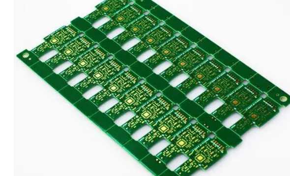
In recent years, 5G and has become the new main force driving the growth of PCB business. From the point of view of product structure, the current PCB market multilayer board still occupies the mainstream position. With the rapid development of electronic circuit industry technology, the integrated functions of components are increasingly extensive, and the high density requirements of PCB are more prominent in electronic products. High-end PCB products such as high multilayer board, flexible board, HDI board and packaging substrate gradually occupy the dominant position in the market.
From the perspective of downstream application field, due to the wide range of applications of PCB products, its periodicity is not affected by a single industry, and it mainly changes with the macroeconomic fluctuations and the overall development of the electronic information industry. Overall PCB growth follows the macro economy.
If the demand is estimated, the price and quantity of PCB for 5G base station will increase, which will strongly drive the demand for PCB use. Guosheng Securities estimates that, based on the comparison between 4G and 5G, 5G base stations may be 1.1 to 1.5 times of the current 4G base stations in terms of the number of 5G base stations, and the number of micro-station construction may exceed 9 million stations. At the same time, it is estimated that the PCB value of 5G base station is about 12,500 yuan, which is about 3 times that of 4G base station in the past.
Electronic industry research judgment, in a period of time in the future, the market share of multilayer board will still be the first place in the market, to provide important support for the overall development of PCB industry; Flexible board, HDI board and packaging substrate and other high technology content PCB proportion will continue to increase, become the mainstream of market development.
According to the 2018 annual report, the optimization of PCB product structure offset the adverse impact of capacity climbing of Nantong plant, and the gross profit margin increased by 0.71 percentage points year-on-year. Packaging substrate revenue increased by 25.52% year-on-year, gross profit margin increased by 29.69%, 3.5 percentage points year-on-year, mainly benefited from the rapid growth of fingerprint and RF module products and the proportion of the increase. The increase in demand for products in the communications sector contributed to a 27.08% year-on-year increase in the revenue of electronic installations.
Shengyi Technology. In the first half of 2019, the number of copper-clad plates sold by Shengyi Technology increased by 4.02% and the number of semi-cured sheets sold by Shengyi Technology increased by 2.13%, but the combined sales revenue of these two products decreased by 2.32%, which also showed the phenomenon of product volume rising and price falling.
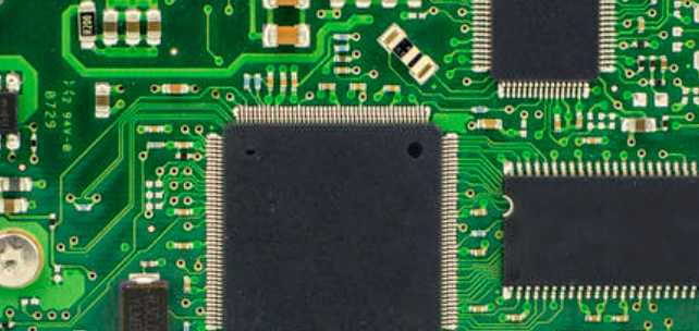
When the power branch is to cross a continuous plane (such as the 3.3V power layer on the OC48 interface card), the power pins and the bypass capacitor themselves do not have to share the same exit diagram to get the lowest inductance and ESR bypass. On mixed-signal PCBS such as the OC48 interface card, special attention should be paid to the wiring of the power branch. Remember to place additional bypass capacitors in a matrix arrangement throughout the card, even near passive devices.
It is worth noting that although the unit price of the products declined, the gross profit margin of Shengyi's copper-clad and bonded sheet business increased, up 4.4 percentage points year-on-year to 22.96%. The increase in gross profit margin was mainly due to the decrease in raw material costs and proper control of unit manufacturing costs, as well as the shipment of some 5G high-frequency copper clad products in the first half of the year.
After the power outlet diagram is determined, automatic wiring can begin. The ATE test contacts on the OC48 card should be defined at logic design time. Make sure the ATE touches 100% of the nodes. In order to achieve an ATE test with a minimum ATE probe of 0.070 in., the breakout via locations must be preserved to ensure that the power layer is not cut off by crossing antipads on the opposite side of the breakout via.

If a power and ground opening (split) scheme is to be used, layer bias should be selected on adjacent wiring layers parallel to the opening. A no-wiring zone is defined on the adjacent layer according to the perimeter of the opening zone to prevent wiring from entering. If wiring must pass through an open area to another layer, ensure that the other layer adjacent to the wiring is a continuous grounding layer. This will reduce the reflection path. Having the bypass capacitor cross the open power layer is good for some digital signal distribution, but bridging between the digital and analog power layers is not recommended because noise is coupled to each other through the bypass capacitor.
Several new automated routing applications are capable of routing high density multilayer digital circuits. The initial wiring phase uses a large 0.050 inch hole spacing in the SMD outlet and takes into account the type of package used. The subsequent wiring phase allows the holes to be positioned close to each other so that all tools achieve the highest spread rate and the lowest number of holes. Because the OC48 processor bus uses an improved star topology, it has the highest priority when routing automatically.


Достаточно загрузить файлы Gerber, BOM и проектные документы, и команда KINGFORD предоставит полное предложение в течение 24 часов.