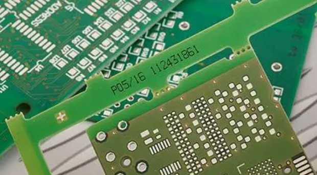
1. Opening principle: Cut aniseed into small pieces according to the size required by MI
2. Inner layer: Paste dry film or printing oil, exposure and etching film inner layer anticorrosion detection is a process of graphic transfer, through the use of film negative, ink/dry film and other media under ultraviolet light, the line graphics required by the customer will be made on the inner layer substrate, and then the unnecessary copper foil etching away, finally made into the inner layer of conductive lines. Pre-treatment: grinding plate inner dry film inner etching inner test + coarse copper plate surface, in order to increase the adhesion of the board and film + clean the board, get rid of the dry film and copper foil covering ink and copper foil covering
3. Plate pressing process: Browning, plate lining, pressing, X-RAY punching, hole and gong edge
4. Drilling process: The role of drilling: to produce a conductive channel on the circuit board that allows the later process to complete the connection between the upper/lower or intermediate circuit layers
5 wet process: copper sedimentation - outer dry film - graphic plating or plate plating - outer layer - corrosion plate - outer layer - corrosion copper detection action: deposit a layer of conductive copper layer on the hole wall of the circuit board insulation, conduction and the connection of the inner line. Outer dry film: stick dry film exposure image plating or plate plating: Function: increase the copper thickness of the circuit board hole \ wire \ face, so as to meet customer requirements. Outer etching: film retreat: The use of strong alkali can make the dry film dissolution or peeling properties of the unwanted dry film from the surface peel or dissolve corrosion plate: the use of bivalence copper ammonium and ion oxidation to the unwanted copper from the plate corrosion tin: The nitric acid in the tin removal water is used to react with tin to remove the tin layer from the board to the outer layer inspection :AOI&VRS takes the PCB image by CCD scanning, compares it with CAM standard graphics by computer and processes the logic of the design specification, marks the bad spots on the circuit board and sends the coordinates of the bad spots to the VRS, and finally confirms the bad spots Location.
6. Wet film process: the main process stations include: printing a layer of photosensitive ink on the outer wire board surface that has been formed and curing it, so as to protect the outer layer and insulation of the circuit board; pre-treatment grinding board, ink printing, oven exposure and image printing, character printing
7. Surface treatment process: Mainly according to the requirements of customers, the copper surface of the circuit board is processed by a layer. The main processing processes are: spray tin: spray a layer of weldable tin surface on the copper surface using hot air welding process. Tin sinking: The use of chemical principles through chemical treatment to deposit tin on the surface of the board. Silking: The depositing of silver on a surface by chemical processes. Gold deposition: The use of chemical principles to deposit gold on a surface. Gold plating: Using the principle of electroplating, through the current and voltage control of gold plating on the surface. Anti-oxidation: The use of chemical principles of an anti-oxidation chemical coated on the surface
8. Molding process: Mainly according to the requirements of customers, a formed circuit board is processed into the size and shape required by customers.
9. Open short circuit test inspection: mainly to check the open circuit and short circuit inspection of the line, as well as the use of visual inspection board quality.
10. Packaging and shipment: the qualified boards will be packaged and finally shipped to customers.
PCB design: Analysis of quality problems in electroplating and etching of printed circuit boards
Etching quality and advanced problem analysis of PCB processing
The basic requirement for etching quality is to be able to remove all layers of copper except below the resist layer, and that is it. Strictly speaking, if it is to be defined, then the etching quality ** includes the consistency of wire width and the degree of side erosion. Due to the inherent characteristics of the present corrosion fluid, not only downward but also to the left and right direction of the etching action, so the side erosion is almost inevitable.
The problem of lateral erosion is one of the etch parameters which is often discussed. It is defined as the ratio of lateral erosion width to etching depth, which is called etching factor. In the printed circuit industry, it varies widely, from 1:1 to 1:5. Obviously, small side etch or low etching factor is desirable.
The structure of the etching equipment and the different composition of the etching solution can affect or control the etching factor or the degree of lateral erosion. The side erosion can be reduced by some additives. The chemical composition of these additives is generally a trade secret, and the respective developers are not disclosed to the outside world. As for the structure of the etching equipment, it will be discussed later.

In many ways, etching quality exists long before the printed circuit board enters the etching machine. Because there is a very close internal relationship between each process or process of printed circuit processing, there is no one is not affected by other processes and does not affect other processes. Many of the problems identified as etching quality actually exist in membrane removal and even in previous processes. The etching process of the outer layer graphics, because it reflects the "pour stream" is better than most of the printed circuit board process, so many problems are reflected in it. At the same time, this is also because etching is a self-laminating, sensitive beginning of a long series of processes in the last link, after which the outer pattern transfer is successful. The more links there are, the more likely there will be problems. This can be regarded as an important aspect of the printed circuit production process.
Theoretically speaking, the printed circuit into the etching stage, in the graphic electroplating process of printed circuit, the ideal state should be: the sum of the thickness of copper and tin after electroplating or copper and lead tin should not be the thickness of the electroplating film, so that the electroplating graphic film on both sides of the "wall" block and embedded in it. However, in reality, the printed circuit board in the world after electroplating, coating pattern is much thicker than the sensitive pattern. The problem arises in the process of plating copper and lead tin, which tends to accumulate laterally because the plating is too high for the sensitive film. A tin or lead tin resist covering the top of the line extends to both sides, forming a "rim" that covers a small portion of the sensitive film underneath the "rim".
The "edge" formed by tin or lead tin makes it impossible to remove the sensitive film when removing the film, leaving a small part of the "residual glue" under the "edge". The "residual glue" or "residual film" left behind the resist "along" will cause no etching. The lines form "copper roots" on both sides after etching, and the copper roots narrow the line spacing, resulting in printed circuit boards that do not meet the requirements of Party A, and may even be rejected. Because the rejection will make the production cost of PCB greatly increased.
In addition, in many cases, due to the reaction and dissolution, in the printed circuit industry, residual film and copper may also form accumulation in the corrosion fluid and blocked in the nozzle of the corrosion machine and acid pump, have to stop processing and cleaning, and affect the efficiency of the work.


