
Контрактное производство электроники под ключ в Китае
Шэньчжэнь, район Баоань, улица Фуюн, улица Фуцяо, район 3, промышленный парк Лонгхуй 6

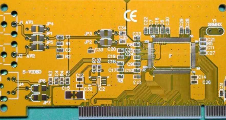
Reviewing the process development of circuit board electronics industry in recent years, we can notice an obvious trend is reflow welding technology. In principle, the reflow process can also be used for conventional inserts, which is commonly referred to as through-hole reflow welding. The advantage is that it is possible to complete all the solder joints at the same time, so that the production cost is minimized. However, temperature sensitive components limit the application of reflow welding, both in cartridge and SMD. Then people turned their attention to selective welding. Selective welding can be used after reflow welding in most applications. This will be an economical and efficient method of welding the remaining inserts and is fully compatible with future lead-free welds.
Process characteristics of selective welding
The process characteristics of selective welding can be understood by comparing with wave soldering. The most obvious difference between the two is that in wave soldering, the lower part of the printed circuit board is completely immersed in the liquid solder, whereas in selective welding, only certain areas are in contact with the solder wave. Since PCB itself is a poor heat transfer medium, it will not heat and melt the solder joints near the components and PCB area during welding. Flux must also be pre-applied before welding. In contrast to wave soldering, the flux is only applied to the lower part of the PCB to be soldered, not the entire PCB. In addition, selective welding is only applicable to the welding of cartridge components. Selective welding is a completely new method. A thorough understanding of selective welding process and equipment is necessary for successful welding.
Selective welding process
Typical selective welding processes include flux spraying, PCB preheating, dipping, and drag welding.
Flux coating process
Flux coating process plays an important role in selective welding. At the end of welding heating and welding, the flux should be sufficiently active to prevent bridging and prevent PCB oxidation. Flux spraying The PCB is carried by the X/Y manipulator through the flux nozzle, and the flux is sprayed on the PCB to be welded. The flux can be sprayed by single nozzle spray, microporous spray and synchronous multi-point/graphic spray. The most important thing for microwave peak selective welding after reflow welding process is accurate spraying of flux. Microjet will never stain the area outside the solder joint. The minimum flux spot graphic diameter of micro-dot spraying is greater than 2mm, so the flux position accuracy of spraying deposited on the PCB circuit board is ±0.5mm, so as to ensure that the flux is always covered on the welding site. The tolerance of flux spraying quantity is provided by the supplier, the technical specification should specify the flux usage, and the 100% safety tolerance range is usually recommended.
Preheating process
The primary purpose of preheating in the selective welding process is not to reduce thermal stress, but to remove the solvent predrying flux, so that the flux has the correct viscosity before entering the solder wave. During welding, the influence of heat brought by preheating on welding quality is not the key factor. PCB material thickness, device package specification and flux type determine the setting of preheating temperature. In selective welding, there are different theories about preheating: some process engineers think that PCB should be preheated before flux spraying; Another view is to weld directly without preheating. Users can arrange the selective welding process according to the specific situation.
Welding technology
There are two different selective welding processes: drag welding and dip welding.
The selective drag welding process is performed on a single small nozzle solder wave. The drag welding process is suitable for welding in very tight Spaces on PCBS. For example: individual solder joints or pins, a single row of pins can be used for drag welding process. The PCB moves on the solder wave of the solder nozzle at different speeds and angles to achieve the best welding quality. To ensure the stability of the welding process, the inner diameter of the welding nozzle is less than 6mm. After the flow direction of the solder solution is determined, the solder nozzle is installed and optimized in different directions for different welding needs. The manipulator can approach the solder wave from different directions, that is, 0° ~ 12° at different angles, so the user can weld various devices on the electronic components. For most devices, the recommended inclination Angle is 10°.
Compared with the dip welding process, the motion of solder solution and PCB board in the drag welding process makes the thermal conversion efficiency better than that in the dip welding process. However, the heat required to form the weld connection is transferred by the solder wave, but the solder wave quality of single nozzle is small, only the solder wave temperature is relatively high, to meet the requirements of the drag welding process.
Example: Solder temperature is 275℃ ~ 300℃, drag speed of 10mm/s ~ 25mm/s is usually acceptable. Nitrogen is supplied in the welding area to prevent oxidation of solder wave, which eliminates oxidation and avoids the generation of bridge defects in the tow welding process. This advantage increases the stability and reliability of the tow welding process.
The machine has the characteristics of high precision and high flexibility, the module structure design system can be customized according to the special Production requirements of customers, and can be upgraded to meet the needs of future production development. The motion radius of the manipulator can cover the flux nozzle, preheating and solder nozzle, so the same equipment can complete different welding processes. The machine's unique synchronous process can greatly shorten the single board process cycle. The manipulator has the ability to make this selective welding with high precision and high quality welding characteristics. First of all, the precision positioning ability of the manipulator is highly stable (±0.05mm), to ensure that the production parameters of each plate are highly repeated and consistent; Secondly, the 5-D movement of the manipulator enables the PCB to contact the tin surface with any optimized Angle and orientation, so as to obtain the best welding quality. The tin wave height measuring needle installed on the manipulator splint device is made of titanium alloy. The tin wave height can be measured regularly under program control. The tin wave height can be controlled by adjusting the tin pump speed to ensure the stability of the process.
In spite of all the advantages mentioned above, the single nozzle solder wave drag welding process also has its shortcomings: the welding time is the longest in the three processes of flux spraying, preheating and welding. And because the solder joints are drag-welded one by one, the welding time will increase greatly with the increase of the number of solder joints, and the welding efficiency can not be compared with the traditional wave soldering process. The situation is changing, however, and multiple nozzle designs can maximize production. For example, double nozzles can be used to double production, and double nozzles can also be used for flux.
The immersion selective welding system has a number of solder nozzle, and the PCB solder joint is designed one to one, although the flexibility is not as good as the manipulator, but the output is equivalent to the traditional wave soldering equipment, the cost of the equipment is relatively lower than the manipulator. Depending on the size of the PCB, a single board or multiple boards can be transferred in parallel, and all spots to be soldered will be sprayed, preheated and welded in parallel at the same time. However, because of the different distribution of solder joints on different PCB, it is necessary to make special solder nozzle for different PCB. The size of the welding nozzle should be as large as possible to ensure the stability of the welding process and not affect the adjacent components on the PCB, which is important to the design engineer, but also difficult, because the stability of the process may depend on it.
The immersion selective welding process can be used to weld 0.7mm ~ 10mm solder joints. The welding process of short pins and small size pads is more stable and the possibility of bridging is small. The distance between adjacent solder joints, devices and welding nozzle should be greater than 5mm.


Достаточно загрузить файлы Gerber, BOM и проектные документы, и команда KINGFORD предоставит полное предложение в течение 24 часов.