
Контрактное производство электроники под ключ в Китае
Шэньчжэнь, район Баоань, улица Фуюн, улица Фуцяо, район 3, промышленный парк Лонгхуй 6

Best PCB Design Method: Six things to consider when selecting circuit board components based on component packaging.
1. Consider component packaging options
Throughout the schematic drawing phase, component packaging and pad pattern decisions that need to be made during the layout phase should be considered. Here are some suggestions to consider when selecting components based on component packaging.
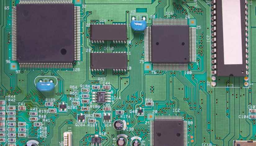
Remember, the package includes the electrical pad connection and mechanical dimensions (X, Y, and Z) of the component, i.e. the shape of the body of the component and the pins that connect the circuit board. When selecting components, you need to consider any mounting or packaging limitations that may exist on the top and bottom layers of the final board. Some components (such as polar capacitors) may have height clearance limitations that need to be taken into account during component selection. At the beginning of the design, you can draw a basic board frame shape, and then place some of the large or location-critical components (such as connectors) that you plan to use. In this way, a virtual perspective of the circiut board (without wiring) can be visually and quickly seen, and relatively accurate relative positioning and component height of the board and components can be given. This will help ensure that the components fit properly into the outer packaging (plastic, case, frame, etc.) after the board is assembled. You can browse the entire board by calling the 3D preview mode from the Tools menu.
The pad pattern shows the actual pad or hole shape of the welded device on the PCB board. The copper patterns on the circuit board also contain some basic shape information. The size of the pad pattern needs to be correct to ensure proper welding and the correct mechanical and thermal integrity of the attached components. When designing the layout of the circuit board, you need to consider how the circuit board will be manufactured, or if it is welded by hand, how the pad will be welded. Reflow welding (where flux is melted in a controlled high temperature furnace) can handle a wide variety of surface attached devices (SMDS). Wave-soldering is generally used to weld the reverse side of the circuit board to secure the through-hole components, but it can also handle some sticker components placed on the back of the circuit board. Usually when this technique is used, the underlying sticker elements must be aligned in a specific direction, and the pad may need to be modified to accommodate this type of welding.
The selection of components can be changed throughout the design process. Determining early in the design process which components should be plated through holes (PTH) and which should be SMT will help with overall board planning. Factors to consider include device cost, availability, device area density and power consumption. From a manufacturing point of view, sticker devices are generally cheaper than through-hole devices and generally have higher availability. For small and medium-sized prototype projects, it is best to choose larger surface stickers or through-hole devices, which are not only convenient for manual welding, but also conducive to better connection of pad and signal in the process of error checking and debugging.
If an existing wrapper is not available in the database, it is common to create a custom wrapper in the tool.
2. Use a good grounding method
Ensure that the design has adequate bypass capacitance and ground plane. When using integrated circuits, make sure to use a suitable decoupling capacitor near the power source end to ground (preferably ground plane). The appropriate capacity of the capacitor depends on the specific application, capacitor technology, and operating frequency. When the bypass capacitor is placed between the power supply and the ground pin, and near the correct IC pin placement, electromagnetic compatibility and susceptibility of the circuit can be optimized.
3. Assign virtual component packages
Print a bill of Materials (BOM) for checking virtual components. Virtual components have no associated encapsulation and are not passed to the layout phase. Create a bill of materials and then look at all the virtual components in your design. The only entries should be power and ground signals, as these are considered virtual components and are only handled specifically in the schematic environment and are not transmitted to the layout design. Unless used for emulation purposes, components displayed in virtual parts should be replaced with components that have encapsulation.
4. Ensure that you have complete bill of materials data
Check for sufficient complete data in the Bill of Materials report. After the bill of Materials report is created, it is carefully reviewed to complete any incomplete device, supplier, or manufacturer information in any component entry.
5. Sort by component label
To facilitate sorting and viewing of the bill of materials, ensure that the component labels are numbered consecutively.
6. Check the excess door circuit
In general, all additional gate inputs should have a signal connection to avoid dangling input ends. Make sure you check for any extra or missing gates and that all unwired inputs are fully connected. In some cases, if the input is suspended, the whole system will not work correctly. Take the circuit board design is often used in the dual operation amplifier for example. If you use only one of the dual-channel opamp IC components, it is recommended that you either use the other opamp as well, or ground the input of the unused opamp and place an appropriate unit-gain (or other gain) feedback network to ensure that the entire component works properly.
In some cases, an IC with suspended pins may not function properly within the target range. The IC will usually work only when the IC device or other gates in the same device are not operating at saturation -- the input or output is close to or at the component power rail. Simulations do not usually capture this situation because simulation models do not generally connect the multiple parts of the IC together to model the suspension connection effect.


Достаточно загрузить файлы Gerber, BOM и проектные документы, и команда KINGFORD предоставит полное предложение в течение 24 часов.