
Контрактное производство электроники под ключ в Китае
Шэньчжэнь, район Баоань, улица Фуюн, улица Фуцяо, район 3, промышленный парк Лонгхуй 6

When hardware engineers are new to multilayer PCB, it is easy to get dizzy. There are often ten or eight layers, and the circuit is like a spider web.
Today, I found several multilayer PCB circuit board internal structure diagram, using three-dimensional graphics to show a variety of laminated structure of PCB diagram internal architecture.
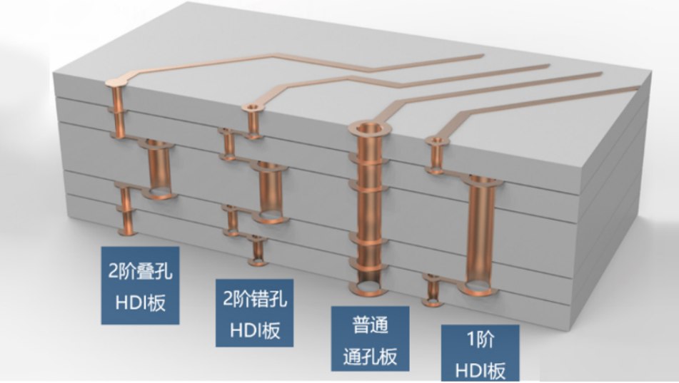
The core of the high-density interconnection board (HDI) is in the through hole
Multi-layer PCB line processing, and single layer and double layer no difference, the biggest difference in the hole process.
Lines are etched out, holes are drilled and then copper plated out, these do hardware development we all understand, do not repeat.
multilayer circuit board, usually through the hole plate, first board, second board, second stack plate these several. Higher level such as the third level board, arbitrary layer interconnection board usually used very little, the price thief expensive, not to discuss.
Under normal circumstances, 8-bit single-chip microcomputer products with 2 layers of through hole plate; 32-bit single-chip level intelligent hardware, using 4-6 layers of through hole plate; Linux and Android level smart hardware, using 6-layer through hole to 8 first-stage HDI boards; Smart phone such compact products, generally use 8 layers of the first level to 10 layers of the second level circuit board.
The most common through-hole

There is only one perforation, from the first layer to the last layer. No matter the external line or the internal line, the hole is pierced, called through hole plate.Through the hole plate and the number of layers does not matter, usually we use 2 layers are through the hole plate, and many switches and military circuit boards, do 20 layers, or through the hole.
The circuit board is drilled through with a drill and copper plated in the holes to create a path.
Note that the inner diameter of the through hole is usually 0.2mm, 0.25mm and 0.3mm, but generally 0.2mm is much more expensive than 0.3mm. Because the drill bit is too thin and easy to break, the drill is also slower. The extra time and drill costs are reflected in the rising price of circuit boards.
Laser hole of high density board (HDI board)

This figure shows the laminated structure of 6 layers of 1 order HDI board. The two layers on the surface are laser holes with 0.1mm bore. The inner layer is a mechanical hole, equivalent to a 4-layer through hole plate, and the outside is covered with 2 layers.
Lasers can only Pierce fiberglass plates, not metal copper. So the outer surface punching will not affect the other lines inside.
After the laser hole is punched, the copper is plated, and the laser hole is formed.
Two layers of laser holes on a 2-stage HDI board

This is a 6 - layer 2 - order staggered HDI board. Usually we use 6 layers of 2 less, most of the 8 layers of 2. There are more layers here, same thing as six layers.
The so-called second order, there are two layers of laser holes.
The so-called wrong hole, is the two layers of laser holes are staggered.
Why stagger it? Because the copper plating is not satisfied, the hole inside is empty, so it can not be directly punched on the above, to stagger a certain distance, and then hit a layer of empty.
Six levels of second order is equal to four levels of first order plus two levels.
Eight levels of second order is equal to six levels of first order plus two levels.
Laminated plate technology is complex and the price is higher

The two layers of laser holes in the staggered plate overlap. The line will be tighter.
The inner laser hole needs to be electroplated and filled, and then the outer laser hole is made. The price is more expensive than the error hole.
Super expensive multi - layer laser hole - stacking of arbitrary - layer interconnectors

Each layer circuit board is a laser hole, and each layer can be connected together. Line the line however you want, punch the hole however you want.
Detail impedance matching
2023-02-15


Достаточно загрузить файлы Gerber, BOM и проектные документы, и команда KINGFORD предоставит полное предложение в течение 24 часов.