
Контрактное производство электроники под ключ в Китае
Шэньчжэнь, район Баоань, улица Фуюн, улица Фуцяо, район 3, промышленный парк Лонгхуй 6

Related concepts of PCB planning
Through hole:
PCB planning once selected through the hole, be sure to deal with it and the surrounding entities of the gap, especially the simple ignored center each layer and through the hole is not connected to the line and through the hole gap, if it is active wiring, can be in the "through the hole number Minimiz8tion" (Via Minimiz8tion) submenu to choose "on" item to active processing. The larger the required load capacity, the larger the required pore size, such as the power layer and the formation used to connect with other layers of the hole is larger.
Screen printing layer:
In order to facilitate the installation and maintenance of the circuit, PCB plans to print on the upper and lower surfaces of the printing board the required logo drawing and text code, such as component label and nominal value, component outline shape and manufacturer's logo, production date and so on. Many beginners planning the content of the screen printing layer, only pay attention to the text symbols placed neatly and beautiful, ignoring the actual PCB circuit board effect. They planned boards where characters were either blocked by components or were rubbed into the soldering area, or where component labels were stamped on adjacent components, all of which made installation and maintenance inconvenient. The correct screen printing layer character placement criteria is: "no ambiguity, see stitches, beautiful and generous".
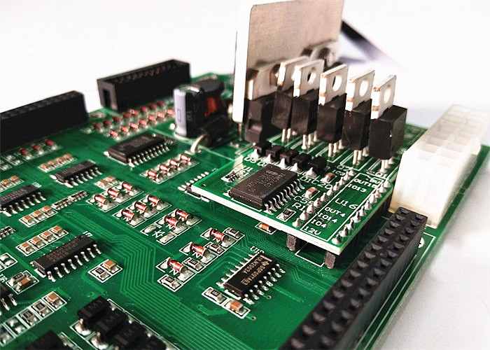
SMD encapsulation:
PCB planning software Protel packaging library has a lot of SMD packaging, namely surface welding equipment. In addition to the small size of this kind of equipment is the biggest feature of single-side distributed pin holes. Therefore, choose this kind of equipment to define the location of good equipment, so as not to "Missing Plns". In addition, the text of this type of component can only be placed with the component surface.
Filling area:
Grid filling area (External Plane) and filling area (Fill)
As the two names indicate, the network filling area is a large area of copper foil treated into a network, the filling area is left intact. Beginner planning process in the computer often can not see the difference between the two, in essence, as long as you expand the picture at a glance. It is because of the usual is not simple to see the difference between the two, so the use of more attention to the difference between the two, to focus on is that the former in the circuit characteristics have a strong inhibition of high-frequency interference effect, suitable for the need to do a large area of filling local, especially some areas as a shield area, cutting area or large current power line is particularly suitable. The latter is mostly used for the general line end or turning area and other small area filling local.
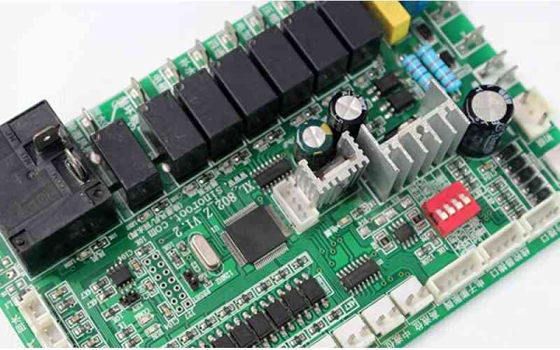
Welding pad:
Pad is the most common contact in PCB planning is also the most important concept, but beginners simply ignore its selection and correction, in the planning of a thousand people to use the circular pad. Select the element of the pad type to comprehensively consider the element's shape, size, placement, oscillation and heat condition, force direction and other factors. Protel gives a series of different sizes and shapes of pads in the packaging library, such as round, square, octagonal, square and positioning pad, but sometimes this is not enough, the need to modify their own. For example, the heat and force larger, larger current pad, can be planned into a "teardrop shape", in the color TV PCB board line output transformer pin pad planning, many manufacturers are using this way.
Generally speaking, in addition to the above, the following criteria should be considered when modifying the pad:
(1) When the length of the shape is inconsistent, the difference between the wire width and the specific side length of the pad should not be too large;
(2) The length of the uneven pad is often used to get twice the result with half the effort when the wiring between the leading angles of the components is required;
(3) The size of each component pad hole should be modified and confirmed according to the thickness of the component pin. The criterion is that the size of the hole is 0.2-0.4mm larger than the diameter of the pin.
All kinds of membranes:
These membranes are not only essential in PCB manufacturing process, but also necessary for component welding. According to the orientation of the "film" and its effect, "film" can be divided into two categories: component surface (or welding surface) welding film (TOp or Bottom and component surface (or welding surface) welding resistance film (TOp or BottomPaste Mask). As the name suggests, the welding film is coated on the welding pad, improve the welding performance of a layer of film, that is, on the green board than the pad slightly larger each light colored round spot. The situation of the solder resistance film is just the opposite, in order to make the board accustomed to wave soldering and other welding methods, the copper foil on the non-plate can not stick to tin, so in the various parts of the plate are coated with a layer of paint, used to prevent these parts on the tin. It can be seen that the two membranes are complementary. From this comment, it is not difficult to confirm the Settings of items like solder Mask En1argement in the menu.
Flying lines serve two purposes:
A network connection similar to a rubber band is used for observation when printed circuit board is planning active wiring. After the component is transferred through the network table and the preliminary layout is made, the crossover condition of the network connection under this layout can be seen by using the Show command. The azimuths of the components are constantly adjusted to minimize such crossover so as to obtain the maximum spread rate of active wiring. This is an important step. In addition, the end of the active wiring, and what network has not been routed, can also be found through the function. Find out the network is not spread, available manual compensation, real compensation can not be used to "fly line" of the second layer of meaning, is in the future printing board with wire connected to these networks. If the circuit board is a mass active line production, the fly line can be considered as 0 oh-resistance resistance with consistent pad spacing resistance components to be planned.
What is HDI and what is HDI circuit board?
2023-02-14


Достаточно загрузить файлы Gerber, BOM и проектные документы, и команда KINGFORD предоставит полное предложение в течение 24 часов.