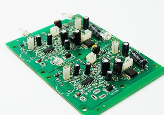
Surface treatment is very necessary for PCB circuit processing. It not only provides a smooth weldable surface for component welding, but also provides protection for the copper conductor of the PCB. Without the protection of surface treatment, PCB copper conductors exposed to the environment will oxidize and deteriorate rapidly, resulting in deterioration of circuit performance. However, increased surface treatment on PCBS also means increased circuit losses. The selection of different surface treatment processes will have different effects on PCB conductor loss, especially for broadband and high-frequency circuits. In order to better understand the effect of surface treatment on loss performance, several transmission lines were processed based on different circuit materials and different surface treatments.
Losses on PCB boards generally increase with frequency, whether or not surface treatment is used. The loss measured by circuit designers on various types of microwave transmission lines such as microstrip line, strip line or ground coplanar waveguide mainly comes from the sum of various signal losses on the PCB, including conductor loss, dielectric loss, radiation loss and leakage loss, which together constitute the insertion loss. The design of the circuit also has an impact on the loss. Good impedance matching of transmission lines, circuit nodes and component welds can reduce the reflected power of the signal and thus reduce the loss. The reflected power can also be obtained by measuring the return loss of the circuit.
Copper is a good conductor and transmission lines and cables using copper have low insertion loss. However, the copper on the PCB dielectric layer cannot always maintain the most flat and smooth surface, especially for small components such as ball matrix packaging (BGA) or SMT. The surface treatment process provides a very smooth mount surface for the installation of small components and provides long-term protection against copper oxidation. Some surface treatments can also effectively protect electroplating through holes (PTHs) in multilayer circuits that realize electrical connections between layers. However, the use of most PCB surface treatments also comes at a cost, with varying degrees of increased insertion loss. This depends on the operating frequency of the circuit and a number of other factors, including the thickness of the media, different transmission line technologies, the way the circuit is wired and the way the surface treatment affects the circuit.

The conductivity of most PCB surface treatment is thinner than that of copper on PCB medium surface, especially in the high frequency band will produce more loss than copper. One exception is silver, which is a good conductor but expensive and usually a very thin layer as a surface treatment. PCB conductor loss is related to frequency mainly because the transmission mode of RF current in the conductor is related to frequency. Due to skin effect, RF current transmission in low frequency band occupies most of the conductor. At high frequencies, RF current will travel along the surface of the conductor, occupying only the outer surface of the conductor. In the high frequency band, the current occupies only a small part of the conductor, which leads to the increase of conductor loss. Surface treatment will have a greater impact on the insertion loss of high frequency PCB.
The effect of surface treatment on PCB insertion loss also depends on transmission line technology. For example, for the microstrip line, which has a high current density at the edge of the conductor, surface treatment will have a significant impact on the conductor loss. For the ground coplanar waveguide circuit, the current density is mainly distributed in the four edge planes of ground wire - signal wire - ground wire, and surface treatment will have a more significant impact on conductor loss.
Selection of surface treatment
There are a number of different surface treatments available for high-frequency circuits, including chemical nickel gold (ENIG), organic solder protection film (OSP), electroless nickel plating, electroless palladium plating, gold immersion (ENIPIG) coating and solder resistant inks. For example, the chemical nickel-gold ENIG electroplates nickel on the surface of the copper conductor of the PCB and then electrogold plating, making nickel as an intermediate layer between copper and gold. Gold is a very good conductor, but a thin layer of gold will be absorbed into the weld when the component is welded to the PCB transmission line or wire and will disappear. The ENIG process uses expensive materials, but it is widely used because it complies with the RoHS standard and provides good protection for PTHs in multilayer circuit assembly.
As a surface treatment process, organic welding film is a popular green lead-free process, which can provide extremely smooth mounting surface for component welding. This surface treatment method is achieved by chemical bath method, which is cheap, but it is not conducive to the protection of PTH. The thickness of the surface treatment cannot be measured when assessing the reliability of the surface treatment process. In addition, even though the life of OSPs can be extended in the best circumstances, OSPs are usually used as transient rather than permanent, final surface treatment processes. Solder proof ink is a polymer material that covers the surface of the copper wire to provide protection against unexpected solder connections and circuit shorting.
How do you compare different types of surface treatments in terms of PCB conductor losses and insertion losses? Different types of transmission line circuits are processed on the same printed circuit board laminate using different surface treatments. The effects of different surface treatments on insertion loss can be compared by measurement and computer simulation.
Another circuit material, 5mil thick, calended copper Rogers RT/duroid6002 circuit board material, was also used to design and fabricate microstrip wire circuits during the evaluation, testing and simulation of surface treatment. It is found that the conductor loss of the microstrip circuit using ENIG is significantly higher than that of the bare copper microstrip circuit in the 40GHz range. However, the same material and the same circuit using the silvery surface treatment process, even if the measurement frequency is increased to 100GHz (using the differential test method), the conductor loss of the microstrip circuit and the bare copper microstrip circuit is very small difference. OSP surface treatments showed similar results, with very little difference even at 100GHz. The conductor loss of microstrip circuit with bare copper structure is about lower than that of microstrip circuit with solderproof ink.
In short, for microstrip and ground coplanar waveguide circuits, the use of bare copper structure has the lowest conductor loss. However, it is not practical to process stable and reliable bare copper structure PCBS. The use of PCB surface treatment technology can provide long term necessary protection. Through measurement and simulation, it can be found that the impact of different PCB surface treatments is different, and the loss of some surface treatments will be lower than others. The measurement of high frequency PCB circuitin the range of 110GHz shows that the conductor loss of circuit from low to high is bare copper structure, tin immersion, ENIPIG, ENIG.


