
Контрактное производство электроники под ключ в Китае
Шэньчжэнь, район Баоань, улица Фуюн, улица Фуцяо, район 3, промышленный парк Лонгхуй 6

From radar to WiFi and walkie-talkies, RF design has become a fixture in our daily lives, thus making RF PCB wiring guidesa fixture in our daily design. Frequencies in the RF range range from thousands to billions of Hz, and these frequencies are found in a large number of analog/mixed-signal devices. The board does not have to be present in a communication device to be classified as an RF circuit, but many of the same design rules will apply.
Rf PCB Wiring Guide: RF Signals and Your Lamination

Wiring RF boards to ensure signal integrity is just as important as designing the correct layer stack and laying the wiring. The transmission line effect in the signal line can be suppressed by placing the correct layering in the PCB.
Although usually discussed in terms of digital signals, when a wire is used as a transmission line, the reflection of signals at impedance discontinuities can affect analog signals. When the propagation delay along the interconnect is greater than a quarter of the oscillation period of the analog signal, you will need to worry about the effect of the transmission line and ensure that the trace impedance matches.
Although the reflected signal in the analog signal trace will decay naturally, the analog trace will be continuously pumped by a harmonic source, and if reflected at an impedance discontinuity, the reflected signal will form a standing wave in the trace. Natural attenuation in signal routing only attenuates the maximum amplitude of resonance, but does not completely eliminate resonance.
Any analog signal resonance on the transmission line can form a standing wave along the line (depending on the geometry), resulting in a high-amplitude electric field that can cause noise in other areas of the board. This problem can be eliminated if the wiring matches the impedance of the source and load components.
So, how do you ensure that the wiring is always impedance matched? First, impedance control design should be used in layer stacking. This ensures that the wiring in the signal layer has a defined value within a specific tolerance. You only need to worry about the impedance of the source and load components matching this value. In other words, if the impedance of a component at the end of the interconnection is different from that of the signal wiring, the impedance of that component must be compensated, not the wiring itself.
Some basic knowledge of RF routing
Since the impedance of the line is very important, your wiring technique should consider all factors related to:
l EMI from other wiring/components, sensitivity to external oscillating magnetic fields, and circuit board radiation
l Decoupling between power supply and ground
l Prevent coupling between RF signals
l Any factor that increases impedance mismatch between wiring, power supply, and load
l Prevent resonances that would strongly radiate to other areas of the board or the external board
l Avoid sharp shapes to eliminate impedance discontinuities
l Use shielded wiring for RF signals
l The RF trace is separated by gaps on the same and other layers
At high frequencies, RF signals may affect other circuits and may be affected by other signals. This is why it is important to protect RF wiring. Key methods include good grounding, shielding and filtering.
While this is a tall order, you can't meet all the requirements all the time. The following points should cause more concern, depending on the specific application of your board.
Although the list of RF PCB wiring guidelines is extensive, here are some important guidelines to consider:
To suppress radiation from the circuit to the power network, the power layer can be surrounded by grounded through-holes. It is also a good idea to place the power plane between the two ground planes, as this will decouple the power plane and ground plane sufficiently across the board.
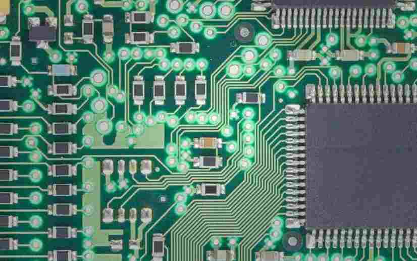
For higher frequency RF circuits, the line carrying the analog signal will need to be very short to prevent transmission line impact. Lines should be spaced as far apart as possible and should not be placed close together for long distances. The coupling between parallel microstrip wiring increases with the increase of parallel wiring distance and the decrease of separation distance.
Once the required routing geometry for a given stack has been calculated, the use of through-holes in the routing should be minimized, as each through-hole increases the impedance of the interconnection. In addition to adding impedance, any short lines left on the through hole will act as a high-frequency resonator. In order to prevent the formation of standing waves in the stub, because the resonant signal in the stub can act as a strong radiator or antenna, the through hole should be drilled in reverse.
If the RF signal line needs to be routed to another layer, two through-holes can be used in parallel to minimize the total additional inductance and impedance. The total impedance and inductance of two through-holes in parallel is half that of a single through-hole. When a bend needs to be placed in an RF signal line due to wiring limitations, you will need to use a bend radius that is at least 3 times the width of the line. This minimizes impedance changes caused by bending the line.
The RF panel acts as a mixed signal device
Unless your RF board is part of a multi-board system, your RF PCB is probably a mixed-signal device. Some devices are exceptions, such as RF amplifiers. Therefore, you will need to consider standard mixed-signal design techniques when using these systems. Some of these devices will be wireless, so wireless design rules will also play a role in your design process.
For RF devices, you may include other analog circuits on the board that support RF components and provide more functionality. In this case, you should try to separate the sensitive RF component from the other analog components to avoid routing the analog return signal under the sensitive RF circuit block.
You will need to follow mixed signal design best practices, including proper division of the ground layer, careful placement of the mixed signal IC, and proper placement of the analog power and grounding components. Your goal should be to reduce the noise in the digital portion so that it is not coupled to the RF analog portion, and vice versa. If you are designing this type of board, note some basic rules for wiring mixed signal PCBS.
Excellent emulation packages capture data from the PCB design package, making it easy to determine the best design choice for a particular application. There are many issues to consider in RF design, as the correct design choice depends largely on the primary operating frequency and whether the RF board is really a mixed signal board.


Достаточно загрузить файлы Gerber, BOM и проектные документы, и команда KINGFORD предоставит полное предложение в течение 24 часов.