
Контрактное производство электроники под ключ в Китае
Шэньчжэнь, район Баоань, улица Фуюн, улица Фуцяо, район 3, промышленный парк Лонгхуй 6

For those who study electronics, it is quite normal to set up a test point on a PCB board, but for those who study machinery, they do not know what the test point is.
Basically, the goal of setting the test place is to test the components on the circuit board are in line with specifications and weldability, for example, if you want to check the resistance on a circuit board is not a problem, the simplest way is to take a universal meter to measure its two ends can know.
But In the mass production of factories have to let you use the meter slowly to measure each wrench on each resistor, capacitance, inductance, and even IC Circuit is accurate, so there is the ICT(in-circuit-test) semi-automatic Test machine is revealed. It uses multiple probes (commonly known as "Bed-Of-Nails" fixtures) to contact all the parts of the wrench that need to be measured at the same time, and then the path through the program-controlled sequence based, parallel auxiliary form along the order to measure the special nature of these electronic parts, Generally, the test of all the parts of the ordinary wrench only takes 1~2 minutes or so to complete, depending on the number of parts on the circuit board, the longer the longer the parts.
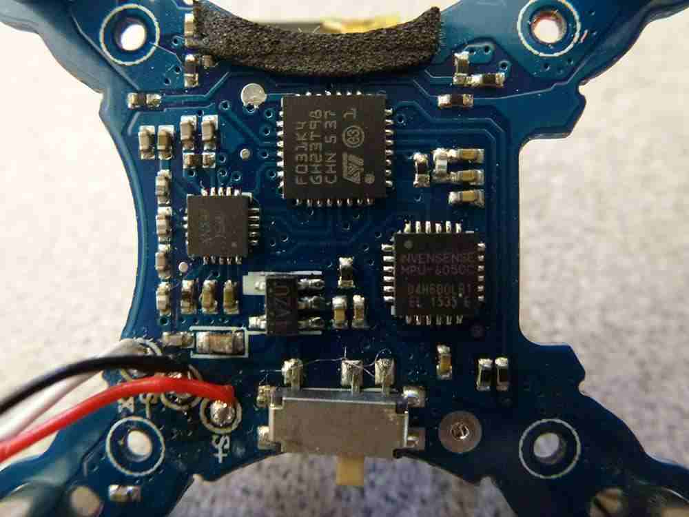
But if these probes directly contact with the wrench on the top of the electronic parts or its welding feet, it is likely to crush a little electronic parts, but counterproductive, so clever engineers created a "test place", at both ends of the parts another lead to a pair of circular points, no welding (mask), The probe that the test is trying to use can be made to touch these dots without having to directly touch the electronic parts being measured.
In the early days when DIP was used on the circuit board, the welding feet of the parts were indeed used as a place for testing. Because the welding feet of the traditional parts are strong enough, they are not afraid to prick the needles. However, bad contact with the probes often leads to misjudgment of things. Because ordinary electronic parts through wave soldering (soldering) or SMT eat tin after this, in the appearance of the solder will generally form a layer of solder paste flux film, the impedance of this film is very high, often lead to the probe contact is not good, so the original production line often visible test operators, Often take an air gun to blow hard, or use ethanol to wipe these demand test places.
In fact, there will be bad contact of the probe where the test is done through wave soldering. Later, after the widespread popularity of SMT, the appearance of test misjudgment has been greatly improved, and the application of test places has also been greatly entrusted with great responsibilities. Since SMT parts are generally weak, it is not possible to bear the direct contact pressure of test probe, so the test places do not need to let the probe directly touch the parts and their welding feet. Not only do we try to take care of the parts without physical damage, but also indirectly greatly improve the reliability of the test, as there are fewer false appearances.
However, with the evolution of science and technology, the size of the PCB circuit board is getting smaller and smaller. It has been a little difficult to squeeze so many electronic parts from the Small circuit board overhead light, so the problem of the space occupied by the test place is often tug-of-war between the preset end and the production end. However, this issue will be discussed when there is an opportunity in the future. The appearance of the test place is generally round, because the probe is also round, it is easier to produce, but also easier to let the adjacent probe closer, so as to increase the density of the needle bed.
1. The use of a needle bed to do circuit testing will have a little innate maximum system on the mechanism, for example: the minimum diameter of the probe has a certain limit, too small diameter of the needle is easy to climb damage.
2. The distance between the needles also has a certain limit, because each needle has to come out from a hole, and the back end of each needle has to burn and weld a flat cable. If the adjacent hole is too small, in addition to the problem of short circuit contact between the needle and the needle, the flat cable is also a big problem.
3. Needles cannot be planted on the side of some tall parts. If the probe is too close to the high part, there will be the risk of collision with the high part, resulting in damage. In addition, due to the high part, the test fixture needle base should be cut to avoid, which also indirectly leads to no way of needle planting. More and more difficult to tolerate on the printed circuit board under all parts of the test place.
4. Because the wrench is getting smaller and smaller, the amount of waste testing place is often taken out to negotiate, and now there is a little loss testing place revealed, such as Net test, Test Jet, Boundary Scan, JTAG, etc.; There are also other test methods to replace the original needle bed test, such as AOI, X-Ray, but so far, it seems that each test can not be 100 percent to replace ICT.
Those experienced in ICT needle planting should consult the appropriate fixture manufacturer, that is, the minimum diameter of the test place and the minimum distance of the adjacent test place. Generally, there will be a minimum expected value and a minimum obtained with experience. But the scale of the manufacturer group requires that the distance between the minimum test place and the minimum test place should not exceed several points, otherwise the fixture is easy to damage.
Knowledge of PCB routing board impedance
2023-02-12


Достаточно загрузить файлы Gerber, BOM и проектные документы, и команда KINGFORD предоставит полное предложение в течение 24 часов.