
Контрактное производство электроники под ключ в Китае
Шэньчжэнь, район Баоань, улица Фуюн, улица Фуцяо, район 3, промышленный парк Лонгхуй 6

In all layers of the PCB board, digital signals can only be routed on the digital portion of the board, and analog signals can only be routed on the analog portion of the board. The ground of low-frequency circuit should be as far as possible to use a single point of parallel grounding, the actual wiring because of difficulties can be partially connected and then grounded in parallel. To realize the segmentation of analog and digital power supplies, the wiring cannot cross the gap between the divided power supplies, and the signal lines that must cross the gap between the divided power supplies should be located on the wiring layer adjacent to a large area.
There are two kinds of electromagnetic compatibility problems caused by power supply and ground in PCB, one is power supply noise, the other is ground noise. According to the PCB board current size, as far as possible to increase the width of the power line, reduce the loop resistance. At the same time, the direction of the power cord and ground wire is consistent with the direction of data transmission, which helps to enhance the anti-noise capability. At present, power and ground level noise can only be set to the default value of the decoupling capacitance by prototype measurements or by experienced engineers using their experience.
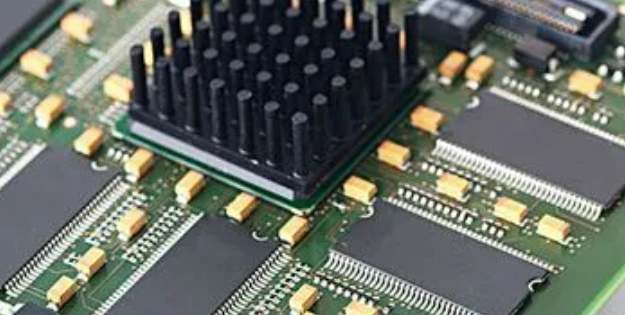
2. Layout rules for Electromagnetic Compatibility (EMC) design of high frequency digital Circuit PCB
The layout of the circuit must reduce the current loop, shorten the line between high-frequency components as much as possible, easily disturbed components should not be too close, input and output components should be as far away as possible.
The position of each functional circuit unit is arranged according to the flow of the circuit, so that the layout is easy to flow signals and keep the signals in the same direction as possible.
The core component of each functional circuit is the center of the layout around it. The components should be arranged evenly, neatly and compact on the PCB, and the lead connection between the components should be shortened as far as possible.
The PCB is divided into separate and rational analog and digital circuits, and A/D converters are placed across the partitions.
One of the common ways of PCB EMC design is to configure appropriate decoupling capacitors in various key parts of PCB board.
(4) Signal integrity (SI) analysis
Signal Integrity (SI) refers to the quality of a signal on a signal line. It is the ability of a signal in a circuit to respond with the correct timing and voltage.
High switching speed of integrated circuit chips (IC) or logic devices, Incorrect layout of terminal components or incorrect wiring of high-speed signals will cause signal integrity problems such as reflection, crosstalk, overshoot, undershoot, ringing and so on, which may make the system output incorrect data. The circuit doesn't work properly or at all.

Signal integrity and design of PCBS
In the design of PCB, PCB designers need to integrate the Layout of components, wiring and what SI problem solution should be adopted in each case, in order to better solve the signal integrity problem of PCB board. In some cases, the choice of IC can determine the number and severity of SI problems. Switching time or edge rate refers to the rate at which the IC state transitions. The faster the IC edge rate, the higher the likelihood of SI problems, and it is important to properly end the device.
A common way to reduce signal integrity problems in PCB design is to add terminal components to the transmission line. In the process of terminating, it is necessary to balance the requirements of the number of components, signal switching speed and circuit power consumption. For example, adding terminal components means that the PCB designer has less space available for wiring, and it is more difficult to add terminal components later in the layout process, as space must be left for new components and wiring. Therefore, in the early stage of PCB layout, it should be clear whether the need to place the terminal components.
Analysis of the difficulties in the manufacture of soft and hard combined plate
Soft and hard combined plate has the stability of hard plate and soft plate can be three-dimensional assembly, the development prospect is very considerable. However, the production process of soft and hard combined board is more complex, and there are some key technical difficulties more difficult to control; The following deep connection circuit will take six layers of single flexible plate weighing structure as an example, for a brief introduction.
1. Basic production process of this combination of soft and hard board:
Analysis of the difficulties in the manufacture of soft and hard combined plate
Soft and hard combined board
2. Design features of this combination of soft and hard board:
Analysis of the difficulties in the manufacture of soft and hard combined plate
3. Difficulties in the production of soft and hard board:
(1) Soft plate:
Hardboard PCB production equipment makes soft board. As soft board material is soft and thin, traction board should be used to carry the soft board across all horizontal lines to avoid scrapping the board.
Pressed PI covering film. Note that PI covering film should be attached locally and fast pressure parameters should be injected. When pressing fast, the pressure should reach 2.45MPa. When pressing fast, it should be smooth and compacted, and the problems such as bubbles and holes should not appear.
(2) Hard plate part:
Hardboard Core for fenestration with PP. The hard plate uses the control of deep milling window, PP to use NO-FLOW PP, NO-FLOW PP can prevent excessive rubber overflow pressing.
Soft and hard combined plate compression expansion and contraction control. As the growth and shrinkage stability of soft plate material is poor, the production of soft plate and pressed PI covering film should be given priority, and the hard plate part should be made according to its growth and shrinkage coefficient.
PCB design of the core problem solution
2023-03-30


Достаточно загрузить файлы Gerber, BOM и проектные документы, и команда KINGFORD предоставит полное предложение в течение 24 часов.