
Контрактное производство электроники под ключ в Китае
Шэньчжэнь, район Баоань, улица Фуюн, улица Фуцяо, район 3, промышленный парк Лонгхуй 6

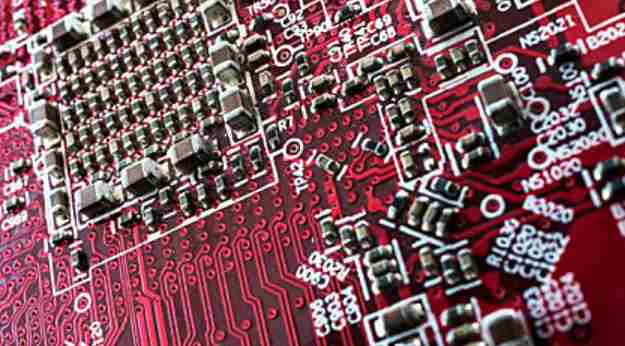
Both radiated and conducted aspects need to be considered in general EMI/EMC design. The former is assigned to the higher frequency part (> 30MHz) the latter is the lower frequency part (< 30MHz). Therefore, we should not only pay attention to the high frequency and ignore the low frequency part. A good EMI/EMC design must take into account the location of devices, PCB laminatedarrangement, important online routes, device selection and so on at the beginning of the layout. If these are not arranged in advance, it will be less effective and increase the cost.
For example, when locating clock generators as close to a slew connector as possible, when taking high speed signals inwards and taking care to slew characteristic impedance matching into the reference layer to reduce reflection, when using a slew rate as low as possible to reduce slew components, When selecting the decoupling/bypass capacitor, check whether the frequency response meets the requirement to reduce the noise of the power layer. In addition, pay attention to the return path of the high frequency current so that the loop impedance is as small as possible to reduce the radiation. The range of high frequency noise can also be controlled by dividing the stratum. Finally, the PCB and chassis ground are appropriately selected.
1. How to choose EDA tools?
In the current PCB design software, thermal analysis is not strong, so it is not recommended to use. For other functions, 1.3.4 PADS or Cadence can be selected with good performance and price ratio. PLD design beginners can use PLD chip manufacturers to provide integrated environment, in the design of more than a million doors can choose a single point of tools.
2. Please recommend EDA software suitable for high-speed signal processing and transmission.
INNOVEDA's PADS work well with analog software for conventional circuit design, which accounts for about 70 percent of applications. In terms of high-speed circuit design, analog and digital hybrid circuit, Cadence should be used as a solution with relatively good performance and price. Of course, the performance of Mentor is still very good, especially in terms of design process management. (Wang Sheng, technical expert of Datang Telecom)

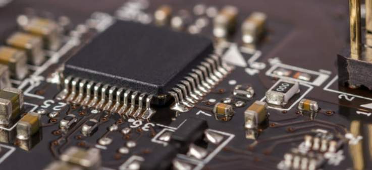
3. Explain the meanings of each layer of PCB board
Topoverlay ---- top silkscreen or top component legend, such as R1 C5,
IC10.bottomoverlay---- Same thing as multilayer----- If you design a 4-layer board and you place a free pad or via, define it as a multilay then its pad will automatically appear on all 4 layers, If you only define it as the top layer, then its pad will only appear on the top layer.
4. What should we pay attention to in the design, wiring and typesetting of high-frequency PCB above 2G?
High frequency PCBS above 2G belong to RF circuit design and are not in the scope of high speed digital circuit design. The RF circuit layout and routing should be considered together with the schematic, because both layout and routing cause distribution effects. Moreover, RF circuit design of some passive devices is achieved by parametric definition, special shape copper foil, so it is required that EDA tools can provide parametric devices, can edit special shape copper foil. Mentor's boardstation has dedicated RF design modules to meet these requirements. Moreover, general RF design requires specialized RF circuit analysis tools, the most famous in the industry is agilent's eesoft, and Mentor's tools have a good interface.
5. What rules should be followed for the design of microstrip for high frequency PCB design above 2G?
In RF microstrip line design, the transmission line parameters need to be extracted by three-dimensional field analysis tools. All the rules should be specified in the field extraction tool.
6. For all digital signal PCB, there is an 80MHz clock source on the board. In addition to the use of wire mesh (ground), in order to ensure sufficient driving capacity, what circuit should be used for protection?
To ensure that the clock drive capability, should not be achieved through protection, generally using clock driver chips. The common concern about clock drive capability is that it is caused by multiple clock loads. The clock driver chip is used to turn one clock signal into several, and the point-to-point connection is adopted. When selecting the driver chip, in addition to ensuring that it basically matches the load and that the signal edge meets the requirements (generally, the clock is an effective signal along the clock), the time delay of the clock in the driver chip should be counted when calculating the system timing.
7. If a separate clock signal board is used, what kind of interface is generally used to ensure that the transmission of clock signals is affected less?
The shorter the clock signal, the smaller the transmission line effect. Using a separate clock signal board will increase the length of signal wiring. And the grounding power supply of the board is also a problem. Differential signals are recommended for long distance transmission. The L number will satisfy the drive capability requirement, but your clock is not too fast to be necessary.
8. 27M,SDRAM clock lines (80M-90M), the second and third harmonics of these clock lines are just in the VHF band, and the interference is very large after high frequency interference from the receiving end. In addition to shortening the length of the line, what are the good ways?


Достаточно загрузить файлы Gerber, BOM и проектные документы, и команда KINGFORD предоставит полное предложение в течение 24 часов.