
Контрактное производство электроники под ключ в Китае
Шэньчжэнь, район Баоань, улица Фуюн, улица Фуцяо, район 3, промышленный парк Лонгхуй 6

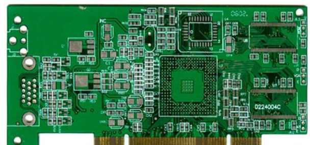
SMT is the abbreviation of Surface Mount Technology, which means surface mount technology in Chinese. Its main role is to install electronic components on the circuit board and welding a processing process, is also the most important link in the manufacturing of electronic products, this kind of processing process is also we often say SMT patch. At present, SMT has been widely used in various industries in the manufacturing of electronic products. Compared with traditional PTH, SMT can greatly improve the production efficiency and shorten the production cycle. In addition to improving the production efficiency, it can also improve the product pass-through rate. Next, I will share with you the equipment and manufacturing process of SMT patch processing, hoping to help you!
I. SMT patch processing includes the following equipment:
1, board machine: board machine is a kind of auxiliary equipment in SMT production and processing, its main role is to put the unmounted PCB board in the SMT board machine automatically send the board to the transmission track, and then through the track to transfer the PCB to the solder paste printing machine track for solder paste brush.
2. Solder paste printing machine: solder paste printing machine is used to print solder paste to the corresponding solder plate on the SMT production equipment in the smt production process. The PCB printed by the solder paste press is convenient for the later patch machine to attach the patch components to the circuit board. Solder paste printing machine is generally composed of PCB clamping, solder paste, printing, transmission and other mechanisms.

3. SPI(3D Solder Paste detector) : SPI is short of Solder Paste Inspection. General people in the industry are directly called SPI(3D solder paste detector). Generally speaking, 70-80% defects in SMT patches come from solder paste printing, so it is necessary to configure an SPI to detect solder paste printing quality after solder paste printing. PCB with poor solder paste printing will be screened before the solder paste printing, so as to improve the straight-through rate after reflow welding. Now more and more 0201 small components need patch welding, so the quality of solder paste printing needs to be higher, and the defects checked after solder paste printing are much lower than the maintenance costs checked after reflow welding.
4. SMT machine: The SMT machine is also known as the "paste machine". In the production line, it is arranged after SPI(3D solder paste detector), and it is a kind of equipment that accurately places the surface mount components on the PCB solder pad by moving the mounting head. As the key and complex equipment in the whole SMT production line, the SMT machine is used to implement the equipment of high speed and high precision. Now, the SMT machine has developed from the early low speed to limited high speed optical alignment, and to multi-function, flexible connection modular development.
5. First-piece detector: First-piece detector is a brand new reform of the traditional PCBA first-piece detection method. It can greatly improve the efficiency of the first piece detection, prevent errors and omissions in the detection process, realize the traceability of the detection process, save manpower and reduce the cost of the first piece detection. Use high LCR tester instead of multimeter, BOM self-check, BOM and coordinate data bidirectional comparison, fast error correction, with screen printing and direction element system automatic optical comparison detection, no manual participation.
6, reflow welding: reflow welding, also known as reflow welding, reflow welding, all refer to the same equipment. Reflow welding has the functions of high production efficiency, less welding defects and stable performance. It is an important welding equipment in SMT manufacturers. The main function of reflow welding is to put PCB board attached with components into the track of reflow welding machine. After temperature rise, heat preservation, welding, cooling and other links, the solder paste from paste to liquid through high temperature, and then to solid after cooling, so as to realize the role of welding between the patch components and PCB board.
7. Plate lowering machine: The plate lowering machine is used at the back end of SMT line, or automatically received into the material frame after reflow soldering PCBA board, without manual board picking operation. And the role of the board machine is similar, one is automatic board, one is automatic board. With automatic lifting/automatic counting/automatic in and out of the material frame and fault alarm function. It can also set the lifting step of the material frame according to the thickness of PCBA.
8, AOI detection: AOI is actually an optical identification system, in today's electronic processing industry has been widely used, and gradually replaced the traditional manual eye inspection. The role of AOI is to use imaging technology to determine whether the object under test meets the standard by comparing whether there is too much difference between the object under test and the standard image. In actual SMT manufacturers, AOI is used to test whether the machining quality and welding quality of electronic components on the circuit board meet the processing standards, so that problems can be found in time and solved in advance. AOI includes online detection and offline detection.
9. X-Ray: With the development of electronic technology, PCBA is ubiquitous in our life. Every electronic product has PCBA, so the application of SMT patch is more and more popular. Due to intellectualization and miniaturization, the size of the chip is getting smaller and smaller, with more and more pins. Ordinary manual detection cannot fundamentally judge the quality of solder joints. AOI detection equipment can only detect the components welded on the surface of PCBA, but cannot detect the reliability requirements of welding quality inside the pins that pass through the board. X-Ray, the official name is X-ray nondestructive testing equipment. Similar to the X-ray machines used in hospitals to take pictures, the main role of electronic manufacturing is to scan and image the inside of the product, especially components such as pin BGA QFN, to detect whether there are abnormal solder joints, such as weak welding, short circuit, etc.
2. SMT patch processing and manufacturing process
PCB loading → solder paste printing → solder paste test (SPI) → Patch → first piece test → Reflow welding →AOI test →PCBA lower plate →X-ray test. That is to say, the first point mentioned above is the equipment used for SMT.
2. What is the preparation work before PCBA processing?
PCBA processing refers to PCB board surface through multiple processes to form PCBA, referred to as PCBA processing. If quality problems occur in a processing link and lead to production suspension, it will bring certain economic losses to the PCBA processing plant. If you want to proceed smoothly in the processing link, it is particularly important to do the corresponding preparatory work before PCBA processing.
1. Data According to the PCBA processing documents provided by the customer, BOM engineers are required to convert them into internal production documents of the company, and at the same time, the documents need to be reviewed. The audit includes the following contents:
(1) Check whether the physical PCB board meets the processing requirements; ② BOM conversion, optimize material description, model, dosage, bit number, packaging, brand, etc.; ③ Convert Gerber files and print processing drawings; (4) According to the related process requirements of each process of PCBA processing; ⑤ Distinguish BOM documents from SMT and DIP;
⑥ Finally, the engineering clerk issues the process documents to the relevant departments and recycling;
2. According to the order plan, confirm in advance whether the steel mesh, fixture and solder paste are ready. If the new steel mesh and jig need to be opened 1 day in advance, the solder paste needs to be thawed 4 hours in advance and stirred 5 minutes before the line;
3. Material inspection: According to the BOM list issued by the engineering, IQC checks whether the material matches the BOM file;
4, components baking: PCB and components are not the original packaging, need to be baked in accordance with the specified temperature and time;
5. Material preparation: According to BOM requirements, SMT patches and DIP plug-in processes need to receive materials from warehouse in advance, SMT needs to load materials on Feeder in advance, and DIP materials need to be formed in advance;
6. Due to the long time of equipment temperature rise and fall, it is necessary to set the wave soldering and reflow welding temperature in advance in the process of wire change.
The above six points are the preparatory work before PCBA processing, which is closely related to the process and efficiency.


Достаточно загрузить файлы Gerber, BOM и проектные документы, и команда KINGFORD предоставит полное предложение в течение 24 часов.