
Контрактное производство электроники под ключ в Китае
Шэньчжэнь, район Баоань, улица Фуюн, улица Фуцяо, район 3, промышленный парк Лонгхуй 6

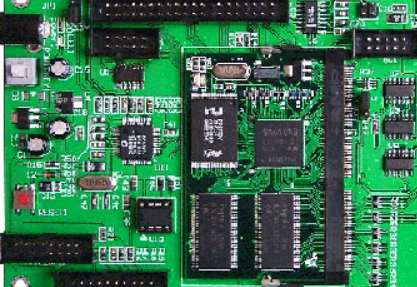
In SMT patch processing, the production materials we use mainly include components, PCB and solder paste. After printing solder paste on PCB board, the components are affixed to the corresponding solder pad of PCB by the SMT machine. Finally, PCBA is formed by reflow welding. Then under what circumstances will SMT production materials affect the welding quality of PCBA? Next, we will share it with you from SMT patch factory -kingford. We hope to help you!
1. Influence of components
When the welding ends or pins of components are oxidized or contaminated, welding defects such as poor wetting, virtual welding and voids will occur in reflow welding. Poor coplanar properties of components will also lead to welding defects such as virtual welding. Therefore, the components shall be stored and baked at specified temperatures in strict accordance with storage requirements.
2. The influence of PCB
The welding quality of PCBA has a direct and very important relationship with the design of PCB pad. If the PCB pad is properly designed, a small amount of skew during SMT fabrication and assembly can be corrected during reflow soldering due to surface tension of the molten solder. On the contrary, if the PCB pad is not designed correctly, even if the mounting position is very accurate, after reflow welding will appear the component position deviation, standing tablet and other welding defects; There is also a certain relationship between the welding quality of PCBA and the quality of PCB pad. When the PCB pad is oxidized or polluted and the PCB pad is damp, welding defects such as poor wetting, false welding, solder ball and cavity will be produced during reflow welding. Therefore, in the inspection of incoming materials, it is necessary to check whether the PCB pad is oxidized and baked at the specified temperature, and whether the matching degree between the component pin and the PCB pad is consistent.

3. The influence of tin paste
The content of metal powder, oxygen content, viscosity, thixotropy and printability of tin paste have certain requirements. If the solder paste metal powder content is high, the reflux temperature of the metal powder with solvent evaporation and splash, if the metal powder oxygen content is high, it will aggravate the splash, the formation of solder ball, but also cause non-wetting and other defects. In addition, if the viscosity of the solder paste is too low or the thixotropy of the solder paste is not good, the solder paste pattern will collapse after printing, and even cause adhesion, and welding defects such as solder ball and bridge will be formed during reflow welding. If the printability of the solder paste is not good, the solder paste is just sliding on the template when printing, in this case, it is not printed on the solder paste. Improper use of tin paste, such as taking out tin paste from the refrigerator and using it directly, will produce water vapor condensation. When reflux temperature rises, water vapor evaporation brings out metal powder. At high temperature, water vapor will oxidize metal powder, splash to form solder ball, and produce poor wetting and other problems. Therefore, this is also the solder paste must be thawed and stirred in advance.
2. What are the contents of SMT patch processing evaluation (DFM) for SMT patch processing?
SMT SMT processing quality assurance premise is derived from PCB board design. Why do you say that? If an SMT patch factory has complete equipment configuration, skilled operators and standardized processes, but the PCB board design received from an order does not meet the requirements of SMT patch processing equipment, I wonder whether it will cause difficulties in processing technology for the factory. The answer is yes, but also increases the manufacturing cost of the processing plant. Therefore, in the early stage when we receive new customer orders, the process department of SMT patch factory should strictly review the manufacturability of PCB board, which will effectively promote customer improvement and product quality improvement.
First, PCB board, overall size, shape, positioning hole and process side review
1, size: the conventional loading capacity of the SMT machine: L460mm*W400mm~L50mm*W50mm; Standard recommendation: 330mm*250mm~50mm*50mm;
2. The outline of all PCB boards must be straight, and there should be no slot in the edge area of PCB board;
3, PCB board shall not be less than two positioning holes, size: ∮1.2-4.0mm;
4, lead-free process: 260℃ ≥10S), after reflow welding can not occur deformation and color change;
5. The safety spacing of PCB peripheral devices is generally 4.75mm (the minimum value of our equipment is 3.5mm);
6, PCB board thickness: equipment capacity (0.38mm~4.2mm; General SMT: > 0.5mm, DIP≥1.0mm (standard 1.6mm bare plate through the furnace) < 1.6mm it is recommended to open a fixture;
7, PCB board warpage: equipment capacity (+ 0.5mm-1.5mm), according to IPC standards, the allowed warpage is 0.7% of the diagonal length of PCB board;
SMC/SMD and THC pad design review
1. SMT inner distance (solder paste process) 1.0201 (0.23-0.25mm) 2.0402 (0.40-0.50mm) 3.0603 (0.70-0.85mm) 4.0805 (1.0-1.20mm) 4.1206 (1.60-2.0mm);
2. DIP plug-in aperture shall be subject to the matching degree between material inspection and corresponding aperture;
Iii. Wiring design, welding pad and printed wire connection review
1, Pad symmetry: for a single shape of the element, the design of the pad should be symmetrical, so as to avoid the phenomenon of standing tablet in reflow welding;
2, the welding disc distance from the position of large copper foil should be greater than 1.8mm; Prevent PCB board surface heating uneven resulting in cold welding phenomenon;
Four, PCB board surface component layout review
1. The distribution of components on PCB should be as uniform as possible; The heat capacity of reflow welding of large mass components is larger, so too concentrated in the layout is easy to cause low local temperature and lead to false welding;
2. Valuable and important components should not be placed at the corners and edges of PCB, or near the connectors, installation holes, slots, cutting of the splicing board (the position of the rib), and corners. These positions are the high stress areas of PCB, which are easy to cause cracking or failure of solder joints and components.
3, components The minimum interval between the device and the V-CUT: 0.5mm, the minimum interval between the stamp hole edge: 1.27mm, the minimum interval between the internal circuit: 0.25mm, the minimum interval between the 1820 components and larger components and PCB edge: 10mm;
4. SMT patch components shall be 5mm away from PCB process edge;
5. Review the spacing between components
1, Chip and Chip pad ≥0.3mm, and IC ≥0.3mm, and shield cover ≥0.5mm, and abnormal device ≥0.5mm;
2. Ensure that there are no interconnected and interfered pads;
Vi. Review of benchmark Mark
1. PCB MARK: No less than 2 boards, 3 boards (300*250mm) are recommended. Specifications: ∮1.0-3.0mm;
2. When the pin number of mounted devices is large and the pin spacing is less than or equal to 0.5mm, it is recommended to set MARK separately for QFP and BGA components;
The above content is provided by kingford, SMT patch factory. For more knowledge about PCB board welding, please visit the official website of kingford Shenzhen Co., LTD


Достаточно загрузить файлы Gerber, BOM и проектные документы, и команда KINGFORD предоставит полное предложение в течение 24 часов.