
Контрактное производство электроники под ключ в Китае
Шэньчжэнь, район Баоань, улица Фуюн, улица Фуцяо, район 3, промышленный парк Лонгхуй 6

kingford is a PCB manufacturer with its own PCB factory and SMT processing factory. We can provide FPC flexible circuit board manufacturing and FPC flexible circuit board processing services.
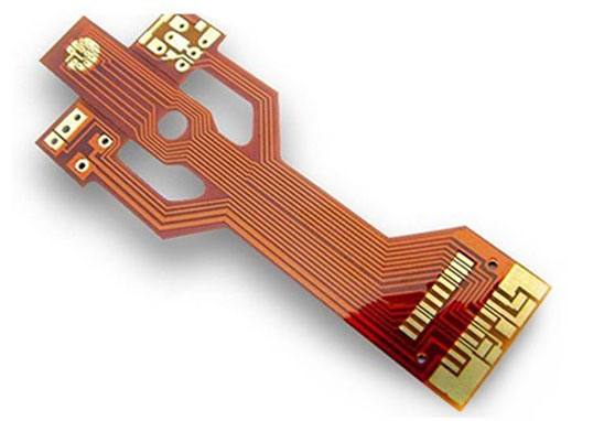
FPC flexible circuit board process capability
Number of rigid/flexible layers: 10/6;
Minimum line width line distance: 3/3mil;
Plate thickness aperture ratio: 12:1;
Hole to conductor distance: 6mil;
Impedance tolerance (Ω) : 10%;
Surface treatment process: lead spray tin, chemical precipitation, precipitation, silver, lead-free spray tin, hard gold plating, soft gold, silver pulp, etc.
FPC Flexible circuit board common types
At present, FPC flexible circuit boards are: single-sided, double-sided, multi-layer flexible circuit boards and rigid and flexible combined circuit boards four kinds.
1. Single-side flexible circuit board is the lowest cost, when the electrical performance requirements are not high printed board. When wiring on one side, one side flexible circuit board should be selected. It has a chemically etched conductive pattern layer, and the conductive pattern layer on the surface of the flexible insulating substrate is calendered copper foil. The insulating substrate may be polyimide, polyethylene terephthalate, arylamide fiber ester and polyvinyl chloride.
2. Double-sided flexible circuit board is a conductive pattern etched on both sides of the insulating base film. Metallized holes connect the two sides of the insulating material to form a conductive path to meet the flexural design and use function. The covering film can protect the single and double-sided wire and indicate the position of the element.
3. Multi-layer flexible circuit board is the single or double-sided FPC flexible circuit board of 3 layers or more layers laminated together, through drilling and plating to form a metallized hole, forming a conductive path between different layers. In this way, there is no need to use complex welding process. Multilayer circuits have great functional differences in terms of higher reliability, better thermal conductivity and more convenient assembly performance. The interaction of assembly size, number of layers and flexibility should be taken into account when designing layout.

4. The traditional rigid and flexible circuit board is composed of rigid and flexible substrate pressed together. The structure is tight and metallized to form conductive connection. If a printed board has components on both sides, rigid flexible circuit boards are a good choice. But if all the components are on one side, it is more economical to use a double-sided flexible circuit board and layer FR4 reinforced material on the back.
5. The hybrid structure of the FPC flexible circuit board is a kind of multi-layer board, conductive layer is composed of different metals. An 8-ply board uses FR-4 as the medium for the inner layer and polyimide as the medium for the outer layer, with leads extending from three different directions of the motherboard, each made of a different metal. Copper alloy, copper and gold are used as independent leads. This kind of hybrid structure is the only feasible solution when the relationship between electric signal conversion and heat conversion and electrical properties are harsh. It can be evaluated by the convenience of the integrated design and the total cost to achieve the best performance-price ratio.
2. How to solve SMT printing leakage and tin deficiency?
kingford has its own SMT SMT processing plant, which can provide SMT processing services for 0201 components with minimum packaging. The SMT processing capacity is 3 to 4 million points/day, supporting incoming material processing and OEM and various PCBA processing forms. Next, how to solve the problem of SMT printing leakage and tin deficiency?
Causes of SMT printing leakage and tin deficiency
1. Solder paste printing principle
The solder paste is extruded into the steel mesh hole by the scraper, so that the solder paste touches the PCB surface and sticks to the PCB surface. The solder paste stuck to the PCB surface overcomes the resistance of the steel mesh wall and transfers to the PCB surface during demounding.
2. Observe, think, and compare
A. Although some areas of the substrate around the pad are covered by steel mesh openings during printing, the solder paste at the bottom of the steel mesh opening is difficult to contact the PCB pad and the surrounding substrate, which is not enough to overcome the resistance of the hole wall (there is only a small amount of solder paste on the pad).
b. There is a ring pit 35 um deep between the pad and the solder shield. Is the solder paste above the pit with the steel mesh opening not in contact with the bottom of the pit?
c. Why are other pads connected with the line not easy to leak?
3. Verification of bare copper plate printing
5 different brands of 4# powder solder paste can stabilize tin in 0.1 thick, 0.28 open diameter round hole (laser + electropolished steel mesh).
SMT processing leakage, less tin bad phenomenon solution
1. Find all the pads that are not connected to the outer circuit, change the size of these pads from the original 0.27 diameter circle to 0.31 diameter circle, reduce the area of deep pits around the pads, make the opening area on the deep pits into the copper foil on the pads, and reduce the gap between the opening area on the deep pits and the bottom of the steel mesh. After the small batch verification is OK, the original steel mesh is used in mass production, and the tin is good under the solder pad which is difficult to lower the tin (increase the area of the solder pad, and no bad tinning is found in batch verification).
2. Reduce the solder resistance thickness of PCB to reduce the influence of the high solder resistance layer on the line near the welding pad. It is recommended that the solder resistance thickness of PCB be less than 25um.
3. The use of new PH steel mesh, the maximum elimination of printing gap, PH steel mesh introduction.
Why choose kingford to manufacture FPC flexible circuit board?
1. Strength guarantee
▪SMT workshop: We have imported SMT machines and several sets of optical inspection equipment, with a daily output of 4 million. Each process is equipped with QC personnel, who can keep an eye on product quality.
▪DIP production line: We have two wave-soldering machines, among which there are more than 10 old employees who have worked for more than three years. The skilled workers can weld all kinds of plug-in materials.
2. Quality assurance, cost-effective
▪ High-end equipment can stick precision shaped parts, BGA, QFN, 0201 materials. Can also template patch, loose material hand.
▪ Sample and size batch can be produced, proofing from 800 yuan, batch 0.008 yuan/point, no start-up fee.
3. Rich experience in SMT and welding of electronic products, stable delivery
▪ Accumulated SMT SMT processing services for thousands of electronic enterprises, involving many kinds of automotive equipment and industrial control motherboard. The products are often exported to Europe and the United States, and the quality can be affirmed by new and old customers.
▪ On time delivery, normal 3-5 days after complete materials, small batch can also be expedited on the same day shipment.
4. Strong maintenance ability and perfect after-sales service
▪ Experienced maintenance engineers can repair all kinds of patch welding caused by bad products, to ensure the connection rate of each piece of circuit board.
▪ 24-hour customer service staff at any time response, the fastest speed to solve your order problems.
Where can circuit board welding be done?
2023-03-16


Достаточно загрузить файлы Gerber, BOM и проектные документы, и команда KINGFORD предоставит полное предложение в течение 24 часов.