
Контрактное производство электроники под ключ в Китае
Шэньчжэнь, район Баоань, улица Фуюн, улица Фуцяо, район 3, промышленный парк Лонгхуй 6

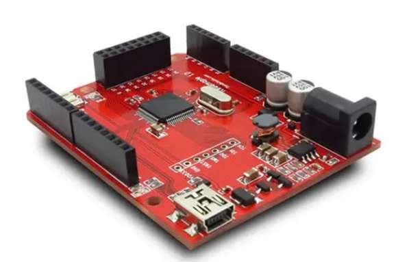
Shenzhen kingford is a professional PCBA processing manufacturerwith more than 20 years of experience in circuit board welding and processing. It has its own PCB board factory and SMT patch factory, which can provide manual welding, SMT patch processing, wave welding processing services, support the processing of materials and samples, OEM and other forms of service.
Circuit board welding processing ability
1. Maximum board card: 310mm*410mm(SMT);
2. Maximum plate thickness: 3mm;
3. Minimum plate thickness: 0.5mm;
4. Minimum Chip parts: 0201 package or parts above 0.6mm*0.3mm;
5. Maximum weight of mounted parts: 150g;
6. Maximum parts height: 25mm;
7. Maximum parts size: 150mm*150mm;
8. Minimum spacing of pin parts: 0.3mm;
9. Minimum ball parts (BGA) spacing: 0.3mm;
10. Minimum ball parts (BGA) ball diameter: 0.3mm;
11. Maximum parts mounting accuracy (100QFP) : 25um@IPC;
12. Patch capacity: 3-4 million points/day.
Circuit board welding precautions
1. After you get the PCB bare board, you should first inspect the appearance to see whether there is short circuit, open circuit and other problems. Then you should be familiar with the schematic diagram of the development board and check the schematic diagram with the PCB screen printing layer to avoid inconsistency between the schematic diagram and PCB.
2. After the materials required for circuit board welding are ready, classify the components into several categories according to their sizes for the convenience of subsequent welding. A complete material list needs to be printed. In the welding process, if you have not finished welding, you will cross out the corresponding options with a pen, so as to facilitate the subsequent welding operation.
Before welding, take ESD measures, such as wearing ESD rings, to avoid electrostatic damage to components. After the equipment required for welding is ready, ensure that the soldering iron tip is clean and tidy. It is recommended to use flat Angle welding iron for initial welding. When welding such as 0603 package components, the iron can better contact the pad and facilitate welding. Of course, for the expert, this is not a problem.
3. When selecting components for welding, welding should be carried out in accordance with the order of components from low to high and from small to large. In order to avoid the larger components welded to the smaller components of the welding inconvenience. Priority is given to soldering integrated circuit chips.
4. Before welding integrated circuit chips, ensure that the direction of chip placement is correct. For the chip screen layer, the general rectangular pad represents the starting pin. During welding, a pin of the chip should be fixed first. After fine-tuning the position of the components, the diagonal pin of the chip should be fixed so that the components are connected to the exact position before welding.

6. Chip ceramic capacitor and voltage regulator diode in voltage regulator circuit have no positive and negative poles, while light-emitting diode, tantalum capacitor and electrolytic capacitor need to distinguish positive and negative poles. For capacitors and diode components, the marked end should be negative. In the package of a patch LED, the direction along the lamp is positive - negative. For the silk-screen marked as diode circuit diagram package components, the vertical end should be placed at the diode negative extreme.
7. For crystal vibration, passive crystal vibration generally has only two pins, and there is no positive or negative division. Active crystal oscillator generally has four pins. It is necessary to pay attention to the definition of each pin to avoid welding errors.
8. For the welding of plug-in components, such as power module related components, the pin of the device can be modified before welding. After the components are placed and fixed, the soldering tin is generally melted on the back through the soldering iron and then the welding pad is integrated into the front. It is not necessary to put too much solder, but the components should be stable first.
9. PCB design problems found during welding should be recorded in time, such as installation interference, incorrect pad size design, component packaging errors, etc., for subsequent improvement.
10, after the completion of welding should use a magnifying glass to check whether there is virtual welding and short circuit.
11, circuit board welding work is completed, should use alcohol and other cleaning agents to clean the surface of the circuit board, prevent the circuit board surface attached to the iron filings to make the circuit short circuit, but also can make the circuit board more clean and beautiful.
2. How to realize PCBA processing program burning?
PCBA processing technology has been increasingly mature, widely used in various intelligent equipment plays a key role. And to let the circuit board to achieve the expected design of the function, in addition to the hardware in place, not to say the matching support of the software program, the program is solidified to IC through the way of burning, so how to achieve PCBA processing program burning?
What is PCBA process burning?
PCBA processing program burning, that is, the process of the program into the chip internal storage space, generally divided into offline burning and online burning.
PCBA processing off-line burning method
Through various adapters compatible with different packages of chips, chip and adapter collocation to achieve the program burning. The adapter itself is a kind of precision fixture, different chips, different packages need to choose different adaptation base.
Now widely used chip packaging such as Emmc to BGA, QFN and other small, flat direction development, and the price of this kind of package adapter is not low.
If there is an error in the production test, it is necessary to remove the chip from the adapter and burn it again in accordance with the prescribed process, which is time-consuming and costly. In the PCBA processing and production, there will be some emergencies, such as the circuit board temperature resistance height is not enough, when disassembling the chip will cause chip deformation, which increases the risk of scrap.
PCBA processing on - line burning method
Online burning is the use of the chip's standard communication bus, such as USB, SWD, JTAG, UART, etc., the interface is generally fixed, burning the need to connect the foot is less. As the interface communication rate is not high, the use of general wire can be completed burning, will not produce high consumption.
Because the online burning is through the wire connection to the program burning, if the production test found error, can immediately on the error of the PCBA backtracking, re burning, and do not need to remove the chip. It not only saves the production cost, but also increases the burning efficiency.
More importantly, the production line is also developing towards automation, more and more manufacturers add ICT, FCT and other functional testing machines to the production line, the use of automatic fixture with online burning production mode can save manual operation in the burning stage, paste the board directly after burning, and then send the PCBA to the test machine test, the whole production process is fully automated. Can greatly improve the production efficiency.
Therefore, in PCBA processing, online burning has significant advantages, and has become one of the important indicators to measure the process accuracy, production efficiency, cost, quality control, scale, capital and other aspects of PCBA manufacturers in the industry.
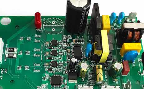
Why choose Deep kingford for circuit board welding?
1. Strength guarantee
▪SMT workshop: We have imported SMT machines and several sets of optical inspection equipment, with a daily output of 4 million. Each process is equipped with QC personnel, who can keep an eye on product quality.
▪DIP production line: We have two wave-soldering machines, among which there are more than 10 old employees who have worked for more than three years. The skilled workers can weld all kinds of plug-in materials.
2. Quality assurance, cost-effective
▪ High-end equipment can stick precision shaped parts, BGA, QFN, 0201 materials. Can also template patch, loose material hand.
▪ Sample and size batch can be produced, proofing from 800 yuan, batch 0.008 yuan/point, no start-up fee.
3. Rich experience in SMT and welding of electronic products, stable delivery
▪ Accumulated SMT SMT processing services for thousands of electronic enterprises, involving many kinds of automotive equipment and industrial control motherboard. The products are often exported to Europe and the United States, and the quality can be affirmed by new and old customers.
▪ On time delivery, normal 3-5 days after complete materials, small batch can also be expedited on the same day shipment.
4. Strong maintenance ability and perfect after-sales service
▪ Experienced maintenance engineers can repair all kinds of patch welding caused by bad products, to ensure the connection rate of each piece of circuit board.
▪ 24-hour customer service staff at any time response, the fastest speed to solve your order problems.


Достаточно загрузить файлы Gerber, BOM и проектные документы, и команда KINGFORD предоставит полное предложение в течение 24 часов.