
Контрактное производство электроники под ключ в Китае
Шэньчжэнь, район Баоань, улица Фуюн, улица Фуцяо, район 3, промышленный парк Лонгхуй 6

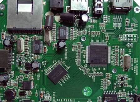
kingford has its own SMT plant, which can provide SMT SMT processing services of 0201 components with minimum package, support incoming material and sample processing and PCBA OEM. Next, we will introduce the core and key points of SMT processing.
SMT processing core and key points
The goal of the SMT process is to produce qualified solder joints. A good solder joint depends on the right pad design, the right amount of solder paste and the right reflow temperature curve. These are the process conditions. Using the same equipment, some manufacturers welding qualified rate is higher, some manufacturers welding qualified rate is lower. The difference is in the process. Reflected in the "scientific, fine, standardized" curve setting, furnace spacing, assembly tooling equipment. And so on. These often take a long time for enterprises to explore, accumulate and standardize. These verified and cured SMT process methods, technical documents, tooling design is the "process", is the core of SMT. SMT process can be divided into process design, process trial production and process control. The core goal is to reduce welding, bridging, printing and displacement problems by designing appropriate solder paste volumes and consistent print deposition. In each business, there is a set of process control points, of which pad design, Stencil design, solder paste printing and PCB support are the key points of process control.
As pad size and chip processing component space continue to shrink, in the printing process, the area ratio of steel mesh opening and the space between the steel mesh and PCB become more and more important. The former is related to the solder paste transfer rate, the latter is related to the consistency of the solder paste printing quantity and printing yield, in order to obtain more than 75% solder paste transfer rate. According to experience, the area ratio of the template opening to the side wall is generally greater than or equal to 0.66: In order to obtain a stable amount of solder paste that meets the design expectations, the smaller the gap between the template and PCB during printing, the better. It is not difficult to achieve an area ratio above 0.66, but it is very difficult to eliminate the gap between template and PCB. This is because the gap between the template and PCB is related to PCB design, PCB warpage degree, PCB support during printing and many other factors. Sometimes subject to product design and use of equipment is uncontrollable, and this is the fine-spaced components.
The key to assembly. Close to 100% welding failures, such as CSPS with 0.4mm pin spacing, multi-row QFN, LGA, and SGA
It has something to do with it. As a result, a number of very effective PCB support tools have been invented to correct PCB bridge curvature and ensure zero gap printing in advanced professional SMT factories.
2. Problems encountered in PCBA manufacturability
Since the 1990s, the development of electronic field changes with each passing day, the design and development of various products and marketing have entered a completely new period. Electronics designers face unprecedented challenges; Customers demand lower prices, higher quality products and shorter delivery times. How to design more functions, smaller volume, higher cost performance, can meet customer needs to the greatest extent of the product, has become the goal of circuit designers. There is always a "gap" between product development and manufacturing due to long-term thinking and operating formulas. Designed products often face the following problems.

1. It does not meet the requirements of PCBA manufacturing capacity and requires a lot of maintenance work, resulting in low product quality and product design changes.
2. The product cannot be manufactured at all, so PCB designers have to start from scratch, which wastes a lot of manpower and material resources and seriously weakens the competitiveness of enterprises in the same industry.
3. Poor product reliability, more customer complaints, large investment in after-sales service, enterprises living beyond their means, shortened product life cycle, and ultimately lead to unsustainable enterprises.
All kinds of problems are related to the manufacturability of PCBA, which is an important factor to be considered in the design of modern electronic products.
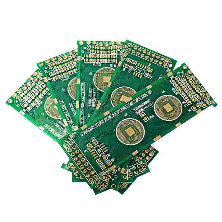
SMT patch processing capability
1. Maximum board card: 310mm*410mm(SMT);
2. Maximum plate thickness: 3mm;
3. Minimum plate thickness: 0.5mm;
4. Minimum Chip parts: 0201 package or parts above 0.6mm*0.3mm;
5. Maximum weight of mounted parts: 150g;
6. Maximum parts height: 25mm;
7. Maximum parts size: 150mm*150mm;
8. Minimum spacing of pin parts: 0.3mm;
9. Minimum ball parts (BGA) spacing: 0.3mm;
10. Minimum ball parts (BGA) ball diameter: 0.3mm;
11. Maximum parts mounting accuracy (100QFP) : 25um@IPC;
12. Patch capacity: 3-4 million points/day.
Why do you choose Shenzhen kingford for SMT processing?
1. Strength guarantee
▪SMT workshop: We have imported SMT machines and several sets of optical inspection equipment, with a daily output of 4 million. Each process is equipped with QC personnel, who can keep an eye on product quality.
▪DIP production line: We have two wave-soldering machines, among which there are more than 10 old employees who have worked for more than three years. The skilled workers can weld all kinds of plug-in materials.
2. Quality assurance, cost-effective
▪ High-end equipment can stick precision shaped parts, BGA, QFN, 0201 materials. Can also template patch, loose material hand.
▪ Sample and size batch can be produced, proofing from 800 yuan, batch 0.008 yuan/point, no start-up fee.
3. Rich experience in SMT and welding of electronic products, stable delivery
▪ Accumulated SMT SMT processing services for thousands of electronic enterprises, involving many kinds of automotive equipment and industrial control motherboard. The products are often exported to Europe and the United States, and the quality can be affirmed by new and old customers.
▪ On time delivery, normal 3-5 days after complete materials, small batch can also be expedited on the same day shipment.
4. Strong maintenance ability and perfect after-sales service
▪ Experienced maintenance engineers can repair all kinds of patch welding caused by bad products, to ensure the connection rate of each piece of circuit board.
▪ 24-hour customer service staff at any time response, the fastest speed to solve your order problems.
What is printed circuit board DFM?
2023-03-14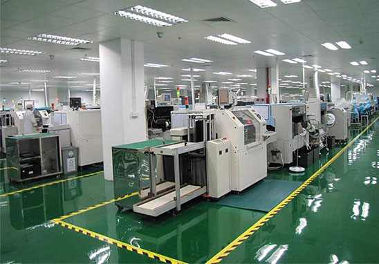


Достаточно загрузить файлы Gerber, BOM и проектные документы, и команда KINGFORD предоставит полное предложение в течение 24 часов.