
Контрактное производство электроники под ключ в Китае
Шэньчжэнь, район Баоань, улица Фуюн, улица Фуцяо, район 3, промышленный парк Лонгхуй 6

Shenzhen kingford is a professional manufacturer of printed circuit board manufacturing circuit board, for many years focused on single, double-sided, multi-layer circuit board production. Can provide impedance board, HDI board, blind hole board and other multi-layer PCB board proofing, small batch production business, the following to introduce the difference between PCB hard board and FPC soft board.
PCB hard board and FPC soft board difference
Rigid PCB: Often used as a motherboard, cannot be bent.
Hard board: PCB (printed circuit board); Flexible board: FPC or FPCB (flexible printed circuit board); Rigid Board: RFPC or RFPCB (Rigid-Flex Printed Circuit Board). A new type of terminal board is used. The hard board section has the same thickness and strength as the PCB circuit board, and can be installed with electronic components and withstand certain mechanical forces. The soft plate section is usually used to achieve 3 D installation. The use of soft plate makes the whole soft and hard binding plate can be partially bent.
Flexible board: FPC also known as Flexible circuit board, can be bent.
Flexible printed circuit board (FPC), also known as flexible circuit board, flexible circuit board, for its light weight, thin thickness, free bending and folding characteristics are favored. Relying on manual inspection, high cost, low efficiency. With the rapid development of electronic industry, circuit board design becomes more and more accurate and intensive. The traditional manual inspection method has been unable to meet the production demand, FPC defect automatic detection has become the inevitable trend of industry development.
2. What are the processing requirements of PCB board?
Shenzhen kingford is a professional manufacturer of printed circuit board manufacturing circuit board, for many years focused on single, double-sided, multi-layer circuit board production. Can provide impedance board, HDI board, blind hole plate and other multi-layer PCB board proofing, small batch production business, the following to introduce the PCB board processing requirements.

PCB board processing requirements
1, indicate the level of PCB printed board processing standards (general enterprises are divided into two levels of standards).
The first level of consumption: only require electrical performance, appearance requirements are not strict.
Secondary industrial category: requirements higher than Grade 1.
For military and other high reliability products, should put forward special processing requirements.
2. Indicate the selected printed board, adhesive prepreg and solder resistance.
3, indicate the PCB manufacturing warpage requirements: SMT PCB requires warpage less than 0.0075mm/mm.
4, PCB processing size: milling (0.2~0.25) mm, punching (0.25~0.30) mm.
5, positioning hole error: ±0.10m.
6, V groove or connection thickness is 13 thickness, error ±0.15mm, Angle 30°/45°±5°
7, the outer ring away from the metallized hole wall at least 0.08~0.15mm.
8. Ensure that the inner layer is well connected.
9, the pattern is accurate, less than 0.25mm line width error is ± (0.05 ~ 0.075) mm.
10. The cereal should be smooth and smooth.
11, BGA holes need to process buried holes or welding resistance layer.
12, the surface of the layer is smooth, the edge of the line should be clear, the character mark is clear, readable, no double shadow.
13, welding resistance to complete the parts required by the enterprise, uniform color.
14. Screen and characters cannot be printed on the pad.
15, the board surface should be clean, there should be no impact on the pcb weldability of debris or glue stains.
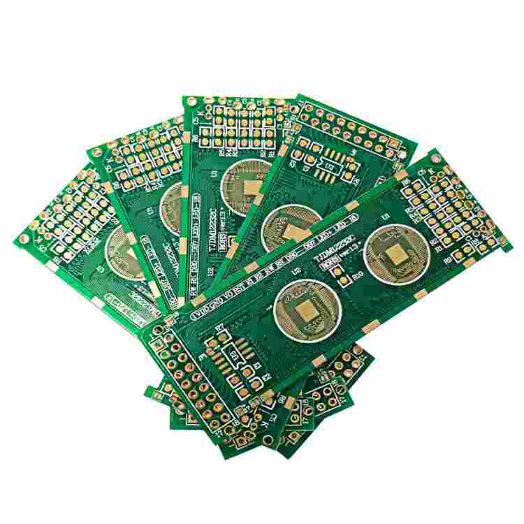
Shenzhen kingford PCB board making ability
Number of layers: 2-40
Plate thickness: 0.2-7.0mm
Maximum copper thickness: 7oz
Finished product size: 650*1100mm
Minimum line width/spacing: 3/3mil
Maximum plate thickness aperture ratio: 12:1
Minimum mechanical drill diameter: 6mil
Hole to conductor distance: 3.5mil
Impedance tolerance (Ω) : ±5%(< 50) ±10%(≥50)
Surface treatment process: OSP, chemical gold plating, chemical nickel palladium gold, tin plating, silver plating, lead-free spray tin, hard gold plating, soft gold plating, gold finger, etc
Materials: FR-4, high TG, halogen-free, high frequency (Rogers, Isola...) , CEM, etc
Our advantages:
PCB boardmaking service started in 1998, with fast delivery ability and quality assurance, can produce high level board, high TG board, HDI board, FPC, rigid torsion board, metal substrate and so on.
Delivery date of PCB allegro and sample:
Double-sided allegro can be completed in 24 hours, multi-layer allegro can be completed in 2-5 days;
Single/double-sided (0.6-1.6mm FR4) delivery time: 3-4 days;
Four-layer plate (0.6-1.6mm FR4) delivery time: 5-6 days;
Six-layer plate (0.8-1.6mm FR4) Delivery time: 7-8 days.
SMT processing core and key points
2023-03-14


Достаточно загрузить файлы Gerber, BOM и проектные документы, и команда KINGFORD предоставит полное предложение в течение 24 часов.