
Контрактное производство электроники под ключ в Китае
Шэньчжэнь, район Баоань, улица Фуюн, улица Фуцяо, район 3, промышленный парк Лонгхуй 6

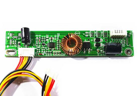
In the process of PCBA processing, there will be a lot of special processes, which will immediately bring the restrictions on PCB board. If PCB board does not meet the requirements, it will increase the difficulty of PCBA welding process, which may eventually lead to welding defects, unqualified boards and other situations. Therefore, in order to ensure the smooth completion of the processing of special technology and facilitate the processing of PCBA, PCB board should meet the manufacturability requirements in terms of size, pad distance and so on. Next, Shenzhen PCBA processing manufacturer -kingford will introduce the requirements of PCBA processing on PCB board.
PCBA processing requirements for PCB board
1. PCB size
PCB width (including board edge) should be greater than equal 50mm, less than 460mm, PCB length (including board edge) should be greater than equal 50mm. Too small size needs to be made into a patchwork board.
2, PCB board edge width
Edge width: > 5mm, plate spacing: < 8mm, distance between pad and plate edge: > 5mm
3. PCB bending degree
Upward bending degree: < 1.2mm, downward bending degree: < 0.5mm, PCB distortion: maximum deformation height ÷ diagonal length < 0.25
4, PCB board Mark point
Mark's shape: standard circle, square, triangle;
The size of Mark; 0.8~1.5mm;
Mark material: gold plated, tin plated, copper platinum;
Mark's surface requirements: smooth surface, no oxidation, no dirt;
Mark's surrounding requirements: there should be no green oil or other obstacles within 1mm, which is obviously different from Mark's color;
Position of Mark: more than 3mm away from the edge of the plate, and no holes or test points similar to Mark can be found in the surrounding 5mm.
5. PCB welding pad
There is no through hole on the patch component pad. If there is a through hole, the solder paste will flow into the hole, resulting in less tin in the device, or tin flow to the other side, resulting in uneven surface of the board, unable to print solder paste.
In PCB design and production, it is necessary to understand some knowledge of PCBA welding process, so as to make the product suitable for production. First understand the requirements of the processing plant, can make the production process more smooth, avoid unnecessary trouble.
This is the PCBA processing of PCB board requirements, in the production of PCB board is not slack, the production of high-quality compliance of PCB board in order to let the board better accept other special processes, and give PCB board life, and inject the soul of function.

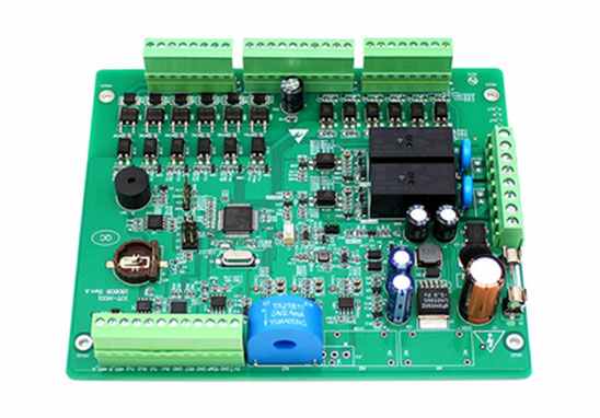
2. Testing skills of circuit board components
The core of electronic equipment is the circuit board, which is welded and assembled by various types of electronic components. If the equipment fails or short-circuits, most of the reasons will be caused by the failure or damage of electronic components. Next, Shenzhen PCBA manufacturer - Shenzhen kingford will introduce the detection skills of circuit board components for your reference.
Test skills of circuit board components
1. Measure the polarity of each foot of the rectifier bridge
Multimeter set R×1k block, black pen bridge pile any pin, red pen has measured the rest of the three feet, if the reading is infinite, then the black pen is connected to the bridge pile output positive pole, if the reading is 4 ~ 10kΩ, then the black pen pin is the bridge pile output negative pole, the other two pins for the AC input bridge pile.
2. Judge the quality of crystal vibration
First, use a multimeter (R×10k stop) to measure the resistance values at both ends of the crystal oscillator. If the resistance value is infinite, it indicates that the crystal oscillator has no short circuit or leakage; Then insert the test pen into the mains jack, pinch any pin of the crystal oscillator with your finger, and touch the other pin to the metal part at the top of the test pen. If the neon bubble of the test pen turns red, it indicates that the crystal oscillator is good; If neon bubble is not bright, crystal oscillator is damaged.
3. Unidirectional thyristor detection
Available multimeter R×1k or R×100 block measurement of any pole of the positive and reverse resistance, if find a pair of pole resistance for low resistance value (100Ω ~ lkΩ), then the black watch pen is connected to the control pole, red pen is connected to the cathode, another extremely anode. There are three PN junctions in thyristor. We can judge its quality by measuring the positive and reverse resistance of PN junctions. When measuring the resistance between the control pole (G) and the cathode [C], if the positive and reverse resistances are zero or infinite, it indicates that the control pole is short circuit or open; when measuring the resistance between the control pole (G) and the anode (A), the positive and reverse resistance readings should be large; when measuring the resistance between the anode (A) and the cathode (C), the positive and reverse resistance should be large
4. Polarity identification of bidirectional thyristor
Bidirectional thyristor has the main electrode 1, the main electrode 2 and the control pole, if the resistance between the two main electrodes is measured with a multimeter R×1k, the reading should be approximately infinite, and the positive and reverse resistance reading between the control pole and any of the main electrodes is only dozens of ohMs. According to this characteristic, we can easily identify the control pole of bidirectional thyristor by measuring the resistance between the electrodes. When the black watch pen is connected to the main electrode 1. The forward resistance measured by the red marker is always smaller than the reverse resistance, according to which we can easily identify the main electrode 1 and 2 by measuring the size of the resistance.
5. Check the quality of the light emitting nixie
The multimeter is set to R×10k or R×l00k, and then the red pen and digital tube (common negative digital tube as an example) of the "ground" leading end is connected, black pen is connected to the other leading end of the digital tube, seven sections should be respectively luminous, otherwise that the digital tube is damaged.
PCBA processing advantages
1. Highly professional: The company focuses on processing samples and small and medium-sized batches, and promises to deliver the materials within 3-5 working days after confirmation.
2. Professional equipment: The company's equipment is tailored for sample and small and medium-sized batch production of advanced equipment, can stick 0201, BGA spacing 0.3MM, QFN, CSP, CON and other components.
3. Professional technology: 100% of technical backbone workers have more than 5 years of work experience, 85% of front-line operators have more than 3 years of work experience.
4. The company implements the 5S and 6σ concepts in daily operation, so as to ensure that the shipment is checked at least 7 times. If the quantity reaches 100PCS, our company promises to pass AOI optical inspection.
5. The company promises that the straight through rate of welding is more than 99%. If customers find welding defects, the company promises to repair them free of charge.
Why kingford?
1. Strength guarantee
▪SMT workshop: We have imported SMT machines and several sets of optical inspection equipment, with a daily output of 4 million. Each process is equipped with QC personnel, who can keep an eye on product quality.
▪DIP production line: We have two wave-soldering machines, among which there are more than 10 old employees who have worked for more than three years. The skilled workers can weld all kinds of plug-in materials.
2. Quality assurance, cost-effective
▪ High-end equipment can stick precision shaped parts, BGA, QFN, 0201 materials. Can also template patch, loose material hand.
▪ Sample and size batch can be produced, proofing from 800 yuan, batch 0.008 yuan/point, no start-up fee.
3. Rich experience in SMT and welding of electronic products, stable delivery
▪ Accumulated SMT SMT processing services for thousands of electronic enterprises, involving many kinds of automotive equipment and industrial control motherboard. The products are often exported to Europe and the United States, and the quality can be affirmed by new and old customers.
▪ On time delivery, normal 3-5 days after complete materials, small batch can also be expedited on the same day shipment.
4. Strong maintenance ability and perfect after-sales service
▪ Experienced maintenance engineers can repair all kinds of patch welding caused by bad products, to ensure the connection rate of each piece of circuit board.
▪ 24-hour customer service staff at any time response, the fastest speed to solve your order problems.


Достаточно загрузить файлы Gerber, BOM и проектные документы, и команда KINGFORD предоставит полное предложение в течение 24 часов.