
Контрактное производство электроники под ключ в Китае
Шэньчжэнь, район Баоань, улица Фуюн, улица Фуцяо, район 3, промышленный парк Лонгхуй 6

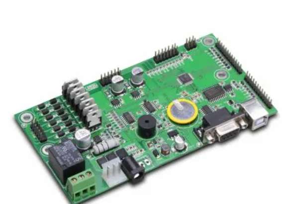
SMT machining is an abbreviation for the process of soldering components onto PCB circuit boards by placing machines and reflow welders. Whether the components can work properly and whether the final circuit board can guarantee normal work and function depends on this. Therefore, process control measurements must be performed prior to SMT machining to optimize PCBA machining and assembly. This will ensure that costly errors are not discovered in the future, reduce product failure rates and protect the reputation of SMT mills.
The process control of PCB assembly mainly involves the implementation of some robust processes during the printing, installation and reflow soldering stages.
Let's dive into some of the details of assembling SMT welding defects. The success of solder paste printing determines whether the overall quality can meet expectations. Therefore, we need to understand and evaluate in detail the quality exceptions that may affect the process.
Before SMT proofing, the following items must be checked:
First, PCB to test the content
1. Whether the PCB light plate is deformed and the surface is smooth;
2. Whether there is oxidation on the circuit board welding plate;
3. Whether the copper coating on the circuit board is exposed;
4. Whether the PCB has been baked for the specified time.

Two, the content of the solder paste should be checked before printing
1. The plates shall not be stacked vertically and shall not collide with each other;
2. Check whether the positioning holes are consistent with the template openings.
3. Whether the tin paste is thawed in advance at room temperature;
4. Whether the selection of solder paste is correct and whether it is expired;
5. Whether SPI solder paste detector has calibration data;
6. Whether the steel mesh and mold are cleaned and whether the flux remains on the surface;
7. Whether to carry out warping test on the wire mesh;
8. Whether the scraping parameters are calibrated and adjusted.
2. Difference between PCBA processing X-ray test and slice test
In PCBA machining, because many high precision circuit boards have a large number of BGA and IC chips, the core parts of the package cannot be directly seen from the surface after welding the internal welded state. Therefore, the PCBA processing plant must be equipped with relevant testing equipment. The main testing equipment for this kind of welding is X-ray.
So what does biopsy do? Its main application is still in the PCB board, PCB board quality is sliced and tested. However, if the SMT patch has a major quality anomaly, special parts of the entire welded board will also need to be sliced and inspected. Both are the internal conditions of welding circuit board, but the application link is different.
What is X-ray detection?
X-rays are used primarily to emit high-energy electrons from a transmitter in a machine to produce X-rays used for sample penetration imaging. Because of the different densities of each structure in the sample, the images shown by X-ray penetrating different objects will have differences in black and white grayscale, showing the location and shape of defects in the sample. The X-ray examination is a non-destructive sample analysis and other tests can be performed at a later date.
Application scenarios of X-ray detection
1. Observe the internal defects of IC packaging parts (line break, holes in packaging materials, cracks, etc.);
2. Observe the welding status of the assembled electronic circuit board (such as air welding, pilling, bridging and other abnormal conditions);
3. Porosity ratio analysis of solder joint;
4. Observe various materials from front, side and bevel angles;
5. Observe the filling of the porous material.
The application of Cross Section Test
It is mainly used for destructive detection of abnormal parts of samples. First, abnormal parts are sampled, then modified with resin seal and cure, then ground and polished, and finally enlarged and examined under a microscope.
Compared to the frequency of using X-ray, the probability of using slice detection is very low and not very common for us.
kingford PCBA processing advantage
1. Highly professional: The company focuses on processing samples and small and medium-sized batches, and promises to deliver the materials within 3-5 working days after confirmation.
2. Professional equipment: The company's equipment is tailored for sample and small and medium-sized batch production of advanced equipment, can stick 0201, BGA spacing 0.3MM, QFN, CSP, CON and other components.
3. Professional technology: 100% of technical backbone workers have more than 5 years of work experience, 85% of front-line operators have more than 3 years of work experience.
4. The company implements the 5S and 6σ concepts in daily operation, so as to ensure that the shipment is checked at least 7 times. If the quantity reaches 100PCS, our company promises to pass AOI optical inspection.
5. The company promises that the straight through rate of welding is more than 99%. If customers find welding defects, the company promises to repair them free of charge.
PCBA proofing process
1. Customers place orders
Customers place orders according to their actual needs of PCBA processing plants, and put forward specific requirements. The processing plant will evaluate its capacity to see if it can fulfill the order. If the manufacturer is sure that they can complete the order within the expected time, then the two parties will negotiate to determine the production details.
2. Production materials provided by customers
After the customer decides to place an order, he shall provide a series of documents and lists to the PCBA processing plant, such as PCB electronic files, coordinate files, BOM list and so on, which must be provided.
3. Purchase raw materials
PCBA processing plant purchases relevant raw materials from designated suppliers according to the documents provided by customers.
4. Incoming material inspection
Before PCBA processing, strict quality inspection is carried out for all raw materials to be used to ensure that they are qualified before being put into production.
5. PCBA production
In the process of PCBA processing, in order to ensure the quality of production, whether it is patch or welding production, the manufacturer needs to strictly control the furnace temperature.
6. PCBA test
The PCBA processing plant conducts rigorous product testing, and the PCB board that passes the test is delivered to the customer.
7. Packaging after sale
After the PCBA processing is completed, the products are packaged and then handed over to the customer to complete the whole PCBA processing.


Достаточно загрузить файлы Gerber, BOM и проектные документы, и команда KINGFORD предоставит полное предложение в течение 24 часов.