
Контрактное производство электроники под ключ в Китае
Шэньчжэнь, район Баоань, улица Фуюн, улица Фуцяо, район 3, промышленный парк Лонгхуй 6

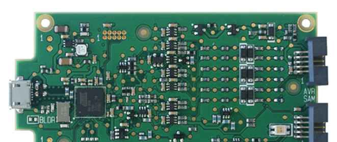
The outer surface of the circuit board usually comes in three colors: gold, silver, and light red. Gold is the most expensive, silver is the cheapest, and light red is the least expensive. So, how to distinguish PCB surface treatment process by color? Next, Shenzhen PCB board manufacturer -kingford will introduce to you.
PCB surface treatment process is identified by color
1. Gold
Gold is real gold, albeit a thin layer, but accounts for nearly 10% of the cost of a board. The purpose of using gold is to facilitate welding and to prevent corrosion. Gold coating is widely used in the parts of the circuit board welding pad, gold finger, connector shrapnel and other positions.
2. Silver
The silver circuit board is called a tin-spray board. Spray a layer of tin over the copper wire to help weld. The tin-spraying plate has no effect on the welded components, but for the welding pad exposed to air for a long time, the reliability is not enough, and long-term use is easy to oxidize and rust, resulting in poor contact.
3. Light red
OSP, an organic welding aid film, is organic rather than metal. It is cheaper than the tin-spraying process. The only effect is to ensure that the inner copper foil will not be oxidized before welding. When the welding is heated, the film evaporates. Osps can weld copper wire and components together when soldering, but are not corrosion resistant. An OSP circuit board, exposed to the air for ten days, will not be able to weld components.

2. What are the advantages of PCB assembly proofing?
In the consultation of many customers, questions about PCB assembling board proofing are often asked. Of course, there are a lot of new customers for PCBA plate proofing is not very understanding. So, what are the benefits of PCB Mosaic proofing?
The advantages of PCB Mosaic proofing
1. In order to improve the qualified rate of electronic products, it is necessary to ensure the quality of PCB, the core component, so it is necessary to produce a small amount of PCB samples in advance to test the performance of products, which can not only improve the production efficiency, but also reduce the production cost.
2, patchwork proofing is an effective measure to reduce production costs. PCB board for the whole PCBA processing process will be much less processes, a whole board, no matter 20 or 10, is to maximize the use of production resources, improve the efficiency of production.
3, PCBA plate proofing for the manufacturer's front-end engineering has great benefits. They can better participate in the production of customers' products, better understand the production and technological difficulties of customers' products; It is of great benefit to the subsequent production quality control. Such early participation helps to control production risks and improve customer satisfaction.
4. It can minimize the quality problems that may be encountered in mass production. After all, ensuring a good reputation is crucial for a manufacturer.
PCB board advantage
Energy production from 2 layers to 14 layers, 14-22 layers can be proofing production.
Minimum line width/spacing: 3mil/3milBGA Spacing :0.20MM
Minimum aperture: 0.1mm Size :610mmX1200mm
Ink: Tamura, Taiyo, Fudoken;
FR4: Shengyi, Kingboard, Harbour, Hongren, Guoji, Hezheng, Nanya,
(Shengyi S1130/S1141/S1170),Tg130℃/ Tg170℃ T g180℃ and other high TG plates)
High frequency plate: Rogers, Taconic, ARLLON;
Surface process: tin spray, lead-free tin spray, gold plating, full plate gold plating, plug gold plating, full plate thick gold, chemical tin (silver), anti-oxidation (OSP) blue glue, carbon oil
Why kingford?
1. Strength assurance
▪ SMT workshop: We have imported SMT machines and a variety of optical testing equipment, capable of producing 4 million pieces per day. Every process is equipped with QC personnel who can keep a close eye on product quality.
▪ DIP production line: There are two wave welding machines. Among them, there are more than ten old employees who have worked for more than three years. Skilled workers can weld all kinds of insert materials.
2. Quality assurance, high cost-effective
▪ High-end equipment can mount precision heterosexual parts, BGA, QFN, 0201 materials. Proofing can be machine paste, also can be hand pendulum.
▪ Samples and large and small batches can be produced. Proofing starting price 800 yuan, batch starting price 0.008 yuan/point, no start-up fee.
3. Rich experience in SMT and welding of electronic products, stable delivery time
▪ Has served thousands of home appliance subsidiaries, involving various kinds of automotive equipment and industrial control motherboard SMT SMT processing services. Products are often exported to Europe and the United States, the quality of new and old customers affirmed.
▪ On time delivery, usually within 3-5 days after the board is assembled, small batch expedited can also be shipped on the same day.
4. Strong maintenance ability and perfect after-sales service
▪ Experienced maintenance engineers are able to repair defective products caused by various welding problems and ensure the connectivity rate of each circuit board.
▪ 24-hour customer service staff will be ready to respond and resolve your order as soon as possible.


Достаточно загрузить файлы Gerber, BOM и проектные документы, и команда KINGFORD предоставит полное предложение в течение 24 часов.