
Контрактное производство электроники под ключ в Китае
Шэньчжэнь, район Баоань, улица Фуюн, улица Фуцяо, район 3, промышленный парк Лонгхуй 6

From PCB design to the completion of all components welding, to become a high quality circuit board, PCB engineers, welding technology, welding workers and many other links to control.
Circuit designers rarely weld circuit boards, unable to obtain rich welding experience, and welding factory workers do not understand the drawing board, just complete the production task, have no mind, more have no ability to analyze the causes of bad welding.
These two aspects of the talent play their own roles, difficult to combine organically. So today I would like to share with you four suggestions of PCB design from the perspective of drawing board.
Four suggestions for PCB design
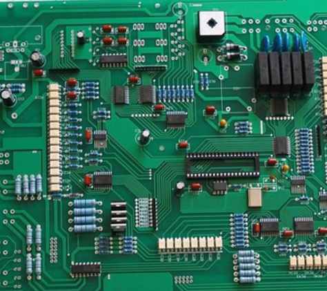
1. About the positioning hole
Four holes (minimum aperture 2.5mm) should be left at the four corners of the PCB board for positioning the circuit board when printing solder paste. I want the center of the X or Y axis to be on the same axis.
2. About the MARK point
The PCB board should be marked with Mark points for placement machine positioning.
Specific position: In the diagonal of the plate, it can be a round or square pad, do not mix with the pad of other devices. If there are devices on both sides, both sides should be marked.
3. Leave 5mm edge
When drawing PCB, no less than 3mm edge should be left in the long side direction for the placement machine to transport the circuit board, and the placement machine cannot mount the device within this range. Do not place patch devices within this range.
For the circuit board of double-sided decoration, consider the secondary reflow welding, the device is rubbed off, the pad is rubbed off and so on.
It is suggested that on the side with fewer chips, the long side should be within 5mm from the side. If it is true that the area of the circuit board is limited, the process edge can be added on the long side.
4, do not directly in the pad over the hole
When the pad is perforated, solder paste will flow into the hole in reflow welding, causing the solder shortage of the device pad and causing virtual welding.
kingfordPCB design ability:
Maximum signal design rate: 10Gbps CML differential signal;
Maximum number of PCB design layers: 40;
Minimum line width: 2.4mil;
Minimum line spacing: 2.4mil;
Minimum BGA PIN spacing: 0.4mm;
Minimum mechanical hole diameter: 6mil;
Minimum laser drilling diameter: 4mil;
Maximum number of pins:; 63000 +
Maximum number of components: 3600;
Maximum number of BGA: 48+.

PCB design service process
1. The customer provides schematic diagram to consult PCB design;
2. Evaluate quotation according to schematic diagram and customer design requirements;
3. The customer confirms the quotation, signs the contract and pays the project deposit;
4. Received advance payment and arranged engineer design;
5. After the design is completed, provide the screenshot of the document to the customer for confirmation;
6. The customer confirmed OK, settled the balance, and provided PCB design materials.
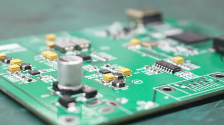
2. How to control the quality of SMT patch processing?
According to statistics, about 30% of SMT processing quality problems are caused by improper control of SMT processing. It can be seen from these data that quality control of SMT processing is very necessary and can indeed achieve the purpose of improving the quality of processed products.
Quality control of SMT patch processing in electronic processing
1. Quality control
Quality control of electronic processing is an important step to ensure product quality and production efficiency in electronic processing plant. Taking the reflow process as an example, although the temperature in the furnace can be controlled by the furnace temperature control system and temperature sensor in the reflow furnace, the actual temperature of the solder joint on the PCBA is not necessarily equal to the preset temperature of reflow welding. SMT patch proofing reflow welder works normally and the temperature control is within the precision range of equipment temperature control. Quality of pcb board. Due to the assembly density and other uncontrollable factors, the furnace temperature curve will fluctuate accordingly. Therefore, the temperature of the reflow welder must be continuously monitored to ensure quality control.
2. Technical requirements for quality control
SMT quality control requires technical personnel to have good measurement knowledge, statistical knowledge, causal analysis ability and in-depth understanding of equipment performance. There are variables on the production line. Equipment aging, personnel adjustment, material quality will affect each other, mutual restraint, making the quality of patch processing products fluctuate.
3. Methods of quality control
At present, in PCBA processing, the introduction of advanced testing equipment for quality control of the production process. In the process of reflow welding, AOI testing equipment is generally used for quality control.
kingford has its own SMT processing plant, which can provide SMT processing services with minimum package 0201 components. The SMT plant is equipped with 3 Fuji high-speed SMT production lines, 2 DIP plug-in production lines, including AOI optical detector, automatic solder paste printing machine, semi-automatic solder paste printing machine, lead-free wave soldering, lead wave soldering, upper and lower 8 temperature zone reflow welding, PCBA functional testing frame, aging, plate loading machine, cleaning tools, etc., and a professional research and development laboratory is also set up. Five professional engineers cooperate with customers to conduct general function testing, test point testing, as well as channel, noise, waveform, drop and temperature testing.


Достаточно загрузить файлы Gerber, BOM и проектные документы, и команда KINGFORD предоставит полное предложение в течение 24 часов.