
Контрактное производство электроники под ключ в Китае
Шэньчжэнь, район Баоань, улица Фуюн, улица Фуцяо, район 3, промышленный парк Лонгхуй 6

Power circuit is an important part of electronic products, power circuit design is directly related to product performance. Next, Shenzhen PCB design company -kingford introduces the PCB design of power supply circuit.
Classification of power supply circuits
The power circuit of our electronic products mainly includes linear power supply and high frequency switching power supply. Theoretically speaking, linear power supply is how much current the user needs, the input will provide how much current; Switching power supply is how much power the user needs, the input provides the amount of power.
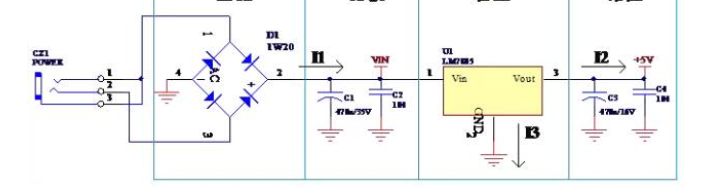
Example of linear power supply circuit schematic
Linear power devices work in linear state, such as our commonly used voltage regulator chips LM7805, LM317, SPX1117 and so on. Figure 1 below is the schematic diagram of the regulated power supply circuit of LM7805.

As can be seen from the figure, linear power supply consists of rectifier, filtering, voltage regulator, energy storage and other functional components. At the same time, linear power supply is generally used as series voltage regulator power supply, and the output current is equal to the input current, I1=I2+I3, I3 is the reference end, the current is very small, so I1≈I3. The reason why we want to talk about current is that in PCB design, the width of each line is not randomly set, but determined according to the current between component nodes in the schematic diagram. The current size and current flow direction should be clear to make the board just right.
PCB design, the Layout of components to compact, to make all the lines as short as possible, to layout components and wiring according to the functional relationship of schematic components. This power supply diagram is the first rectifier, then filtering, filtering after voltage regulation, voltage regulation after energy storage capacitor, after flowing through the capacitor to the circuit behind the electricity.
After the power supply is rectified, it directly comes to the input foot of the voltage regulator chip, and then the voltage regulator capacitor. The filtering effect of the capacitor here is much worse, and the output has problems. The picture on the right is a good one. We should not only consider the flow direction of the positive power supply, but also consider the ground reflux problem. Generally speaking, the positive power line and the ground reflux line should be as close to each other as possible.
When designing PCB of linear power supply, attention should also be paid to the heat dissipation problem of the power regulator chip of linear power supply. How does the heat come? If the voltage regulator chip front end is 10V, the output end is 5V, and the output current is 500mA, there is a 5V voltage drop on the regulator chip, and the heat generated is 2.5W; If the input terminal voltage is 15V, the voltage drop is 10V, the heat generated is 5W, therefore, we cloth the board is to set aside enough heat dissipation space or reasonable heat sink according to the heat dissipation power. Linear power supply is generally used in relatively small pressure difference, the current is relatively small occasions, otherwise, please use switching power supply circuit.
Schematic diagram of high frequency switching power supply
Switching power supply is to use the circuit to control the switching tube for high-speed on-off and cut-off, generate PWM waveform, through the inductance and continuous current diode, the use of electromagnetic voltage conversion. Switching power supply has large power, high efficiency and small heat. We generally use circuits such as LM2575, MC34063, SP6659 and so on. In theory, switching power supply is equal at both ends of the circuit, the voltage is inversely proportional, the current is inversely proportional.

When PCB design of switching power supply, it is necessary to pay attention to the place is: the input point of the feedback line, the continuation diode is to whom the continuation. As can be seen from Figure 3, when U1 is switched on, the current I2 enters the inductor L1. The characteristic of the inductor is that the current cannot be generated or disappeared suddenly when it flows through the inductor. The change of the current in the inductor has a time process. Under the action of pulsed current I2 flowing through the inductance, part of the electric energy is converted into magnetic energy, and the current increases gradually. At a certain time, the control circuit U1 turns off I2. Due to the characteristics of inductance, the current cannot disappear suddenly, at this time the diode plays a role, it takes over the current I2, so it is called continuous current diode. The continuing current I3 starts from the negative end of C3 and flows into the positive end of C3 through D1 and L1, which is equivalent to a pump and increases the voltage of capacitor C3 by using the energy of inductance. There is also the problem of the input point of the feedback line of voltage detection, which should be fed back after filtering, otherwise it will make the output voltage ripple larger. These two points are often ignored by many PCB designers, who think that the same network can be connected in different places. In fact, the connection places are different, which has a great impact on performance.
Why do we want to talk about the schematic principle in detail? Because the schematic diagram contains a lot of information to draw PCB, such as the access point of the component pin, the current size of the node network, etc. After reading the schematic diagram clearly, PCB design will not be a problem. The LM7805 and LM2575 circuits represent the typical layout circuits of linear power supply and switching power supply respectively. When making PCBS, the layout and wiring of these two PCB diagrams are acceptable. The only difference is that the products are different and the circuit boards are different.
All change from its Zong, so the principle of the power circuit and the way of cloth are so, and every electronic product can not be separated from the power supply and its circuit, therefore, learn to pass the two circuits, the other is also in the chest.
Shenzhen PCB Design Company
kingford is a professional PCB design company engaged in electronic products layout layout design, mainly undertake multi-layer, high density PCB design and circuit board design proofingbusiness. Proficient in the use of market mainstream PCB design software, professional and efficient communication to ensure the progress of PCB design, to help you seize the market opportunity one step earlier!
How to optimize circuit board design
2023-02-28


Достаточно загрузить файлы Gerber, BOM и проектные документы, и команда KINGFORD предоставит полное предложение в течение 24 часов.