
Контрактное производство электроники под ключ в Китае
Шэньчжэнь, район Баоань, улица Фуюн, улица Фуцяо, район 3, промышленный парк Лонгхуй 6

This paper mainly introduces the PCB window, first introduces the window and bright copper in PCB design, then introduces how to realize the PCB wire window on tin, finally describes the PCB design how to set the steps of wire window, follow the small series together to understand.
What is pcb fenestration
The wires on PCB are covered with oil, which can prevent short circuit and damage to the device. The so-called window is to remove the paint layer on the wire, so that the wire can be exposed to tin.
As shown in the picture above, it is through the window. PCB window opening is not rare, the most common may be the memory strip, the students who have dismantled the computer know that the memory strip has a gold finger, as shown in the picture below:
The gold finger here is opening the window, plug and play.
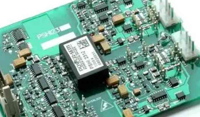
There is also a very common function of the window, is the late hot tin to increase the thickness of copper foil, convenient for excessive current, which is common in the power board and motor control board.
PCB design window and bright copper
In the design process, we often meet customers' requirements for opening Windows and brightening copper. However, because the customers have little knowledge or we are not very clear about this process, the communication is very troublesome. In our design, customers often encounter the need to add shielding cover, plate edge local bright copper, over hole welding, IC heat sink back exposed copper, stealing tin pad and so on. According to the actual situation, let's take a look at some pictures to explain.

1. Shielding cover
If the customer needs to add a shielding cover, then what we need to do is to add soldmask with a width of at least 1mm. Whether to add steel mesh needs to be confirmed with the customer. At the same time of adding soldmask, we need to spread the ground network copper skin in the area of adding soldmask, which must cover the soldmask plane, otherwise the substrate (FR4, etc.) will be exposed. Do not pass over soldmask for other non-terrestrial networks. Add the soldmask area to the pcb effect and the yellow copper will be revealed. Unadded areas will be covered by solder resistance.
2, welding resistance window hole
In the design, we often hear the whole plate plug hole or local plug hole. When adding holes, we note that the plug hole company's name is generally BGA, whereas those without BGA are welding resistance window holes (our company's specification). The general company code for holes over 12mil must be welded to the window openings.
3, IC cooling pad
In general, add welding resistance window on the back of IC heat dissipation pad (add the back soldmask larger than the surface or equal to the surface of the surface of the pad) and ground holes, and cover the ground copper welding on the back, so as to better spread the surface heat through the ground hole to the back of the copper skin better out.
4. Steal tin pad
In wave soldering, in order to solve the tin connection problem caused by the close spacing of pads, we will use tadpole shape tin stealing pads. Note When adding the solder resistance, add a copper skin of the same size as the solder resistance.
How to realize PCB wire opening window on tin
When the multi-channel relay is closed and switched on, the current increases greatly. In order to ensure the actual effect, the welding resistance layer -- green oil layer -- on the current line is expected to be removed when the current line is widened. After the board is made, tin can be added to it and the line can be thickened so that a larger current can pass through.
The implementation method is as follows:
Draw this wire in the toplayer (or bottomlayer depending on which layer the preset wire is in) layer, and then draw a line that coincides with this wire in the topsolder (or bottom solder) layer.
How to set the wiring window in PCB design
CB design can set a wire opening window in the TOP/BOTTOM SOLDER layer.
Top/bottom solder green oil (top/bottom solder green oil) : Install solder green oil on the top/bottom to prevent solder on the copper foil and keep insulation.
Welding resistance green oil window can be set on the welding pad, through hole and non-electrical wiring of this layer.
1. The welding pad will open a window by default in PCB design (OVERRIDE: 0.1016mm), that is, the welding pad is exposed to copper foil, the outer expansion is 0.1016mm, and the tin will be raised during wave soldering. No design changes are recommended to ensure weldability;
2. The overhole will be windowed by default in PCB design (OVERRIDE: 0.1016mm), that is, the overhole copper foil will be expanded by 0.1016mm, and the tin will be raised during wave soldering. If the design is to prevent SOLDER from passing through the hole, do not expose copper, you must check the PENTING option of SOLDER MASK (solder window) to close the pass through the hole window.
3. In addition, non-electrical wiring can also be carried out on this layer separately, so the welding green oil can be opened accordingly. If it is on the copper foil wire, it is used to enhance the ability of wire current, solder treatment; If it is on the non-copper foil wire, it is generally designed to do identification and special character silkscreen printing, which can save the production of character silkscreen layer.
Multi-person online collaborative PCB design
2023-02-27


Достаточно загрузить файлы Gerber, BOM и проектные документы, и команда KINGFORD предоставит полное предложение в течение 24 часов.