
Контрактное производство электроники под ключ в Китае
Шэньчжэнь, район Баоань, улица Фуюн, улица Фуцяо, район 3, промышленный парк Лонгхуй 6

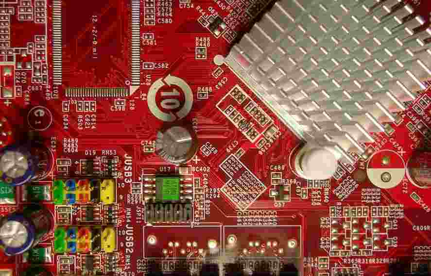
Usually on a circuit, or a product is not so much, for example, in the TV this product, from the power supply, 220V there is an alternating current, after the transformer is DC, and then it is divided into digital and analog, like the sound processing part, there is a clear division, booster circuit power, modern society to digital, There's a lot of digital signal in there, mostly digital. A little grounding, in low frequency circuits, does not have much effect between wiring and components. Generally, circuits with frequencies less than 1MHz are grounded at one point. In high frequency circuit, the influence of parasitic capacitance and inductance is great. Generally, a circuit with a frequency greater than 10MHz is grounded at multiple points. The specific use of which connection depends on the specific situation. These are the PCB design must understand the content, but also important data. How to partition in PADS is described later in this article.
The following is the division of land under the Internet for reference:
Digitally: Also called logically, is the zero potential reference point of a digital circuit.
Hot ground: Switching power supply does not need to use transformers, and the "ground" of its switching circuit is related to the mains power grid, namely the so-called "hot ground". It is charged, and the graphic symbol is:
Cold ground: the high-frequency transformer of the switching power supply will isolate the input and output terminals; And because its feedback circuit is usually photoelectric coupling, it can transmit feedback signal and isolate the ground of both sides. So the output ground is called cold ground, it's not charged.
Signal ground, also known as reference "ground", is the reference point of zero potential, is also a common section of the circuit signal loop, graphic symbol
Dc ground: DC circuit "ground", zero potential reference point.
Alternating ground: the neutral line of alternating current. Should be distinguished from ground wire.

Power ground: zero potential reference point of large current network devices and power amplifier devices.
Analog: Zero potential reference point for amplifiers, sample retainers, A/D converters, and comparators.
Protected ground is a connection mode set up to protect the safety of personnel. One end of the ground wire is connected to electrical appliances, and the other end is reliably connected to the earth. Ground shield wire grounding in sound system: in order to prevent interference, the metal housing is connected with the signal ground, which is called shield grounding. Audio special professional audio in order to prevent interference, in addition to the shield, but also need to be connected with audio special. The grounding device should be specially buried, and should be connected with the corresponding grounding terminal of the isolation transformer and shielded voltage regulator power supply as a special audio grounding point in the audio control room.
Treatment of different ground wires
System floating ground, is the grounding of each part of the system circuit floating up, not connected with the earth. PCB layout training of this connection, has a certain anti-interference ability. However, the insulation resistance between the system and the ground shall not be less than 50M; , once the insulation performance is reduced, it will bring interference. The system is usually floating and the housing is grounded, which can enhance the anti-jamming ability and make it safe and reliable. In high demand circuits, digital and analog ground must be separated. Even for A/D and D/A converters, it is best to separate the two lands on the same chip and connect the two lands only at the system point. Floating and grounding.
Meaning and design principle of PCB multilayer board
PCB's are single - sided, double - sided and multilayer. For simple electrical appliances such as radios, use single - sided PCB's. However, with the progress of The Times, both function and volume, electronic products need to be updated. For multifunctional, small size electronic products, single and double sided PCB can not fully meet the requirements, but must use multi-layer PCB.
Multilayer PCB has many advantages, such as: high assembly density, small size; The wiring between electronic components is shortened, the signal transmission speed is fast, and the wiring is convenient; Good shielding, etc. There is no limit to the number of layers of multilayer boards. At present, there are more than 100 layers of PCB, and the common ones are four and six layers of boards.
Multilayer board in the design, each layer should maintain symmetry, and it is best to even copper layer, if not symmetrical, easy to cause distortion. The wiring of multilayer board is carried out according to the function of the circuit. When wiring the outer layer, more wiring is required on the welding surface and less wiring on the component surface, which is conducive to the maintenance and troubleshooting of printed board. In routing, the power layer, ground layer and signal layer should be separated to reduce the interference between the power, ground and signal. The lines of the adjacent two layers of printed boards should be perpendicular to each other as far as possible or diagonal lines, curves, not parallel lines, in order to reduce the interlayer coupling and interference of the substrate.
Compared with single-sided and double-sided PCB, which layers are composed of? What does each layer represent and what is its use? Multilayer PCB is mainly composed of the following Layers: Signal Layers(signal layer), InternalPlanes(internal power supply), Mechanical Layers(mechanical layer), Masks(welding resistance layer), Silkscreen(Silkscreen), and System(system working layer).
The signal layer is divided into top layer, middle layer and bottom layer, which is mainly used to place various components, or for wiring and welding. The internal power layer, also known as the internal power layer, is dedicated to arranging power cables and ground cables. The mechanical layer is generally used to place the indicative information about board making and assembly methods, such as the physical size line of the circuit board, data data, hole information, etc. The solder stop layer also has a top layer and a bottom layer on which the pad or other object placed is a copper-free area. The screen printing layer is mainly used to draw the outline of the component, the number of the placed component or other text information, while the system working layer is used to display the information that violates the design rule check.

How to design pcb window opening
2023-02-27


Достаточно загрузить файлы Gerber, BOM и проектные документы, и команда KINGFORD предоставит полное предложение в течение 24 часов.