
Контрактное производство электроники под ключ в Китае
Шэньчжэнь, район Баоань, улица Фуюн, улица Фуцяо, район 3, промышленный парк Лонгхуй 6

The main reasons for poor wetting in SMT patch processing plants are:
1. The surface of the welding area is contaminated, the surface of the welding area is stained with flux, or metal compounds are generated on the surface of the patch element. Can cause poor wetting. Such as sulfide on the surface of silver, tin has oxides on the surface will produce poor wetting.
2, when the residual metal in the solder exceeds 0.005%, the activity of the flux is reduced, and poor wetting will also occur.
3, wave soldering, there is gas on the surface of the substrate, but also easy to produce poor wetting.
SMT patch processing plant to solve poor wetting methods are:
1. Strictly implement the corresponding welding process.
2, PCB board and component surface to do a good job of cleaning.
3, select the appropriate solder, and set a reasonable welding temperature and time.

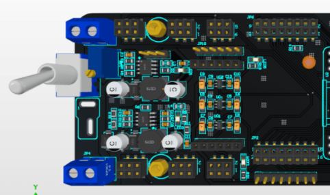
2. PCBA board inspection project standard of SMT patch factory workshop
SMT workshop PCBA board inspection project standard
01. Air welding of solder joints for SMT parts
02. Cold welding of solder joints of SMT parts: gently dial the pin of the part with a toothpick. If it can be moved, it will be cold welding
03.SMT parts (solder joints) short circuit (tin bridge)
04.SMT parts are missing
05.SMT parts are wrong
06.SMT parts with opposite polarity or wrong resulting in combustion or explosion
07. Multiple SMT parts
SMT patch processing
08.SMT parts turning: text face down
09.SMT parts stand side up: chip components no more than 3mm in length and 1.5mm in width no more than five (MI)
10.SMT parts tombstone: the end of the chip element is warped
11. Foot offset of SMT parts: Side offset is less than or equal to 1/2 of the width of weldable end
12. Float height of SMT parts: distance between bottom of components and substrate < 1mm
13.SMT feet high warping: the height of warping is greater than the thickness of parts feet
14.SMT parts heel not flat stick heel not eat tin
15.SMT parts cannot be identified (blurred printing)
16.SMT parts foot or body oxidation
17.SMT parts body damage: capacitor damage (MA); Resistance breakage less than 1/4(MI) of component width or thickness; Length of IC breakage in any direction < 1.5mm(MI), revealing internal material (MA)
18.SMT parts shall be supplied by non-designated supplier: according to BOM, ECN
19. Solder tip of SMT parts: the height of solder tip is greater than the height of part body
20.SMT parts eat too little tin: the minimum solder joint height is less than 25% of the solder thickness plus the height of the weldable end or solder thickness plus 0.5mm, the smaller is (MA
21.SMT parts eat too much tin: the maximum solder joint height exceeds the pad or climbs to the top of the welding end cap of the metal coating is acceptable, solder contact element body (MA)
22. Tin balls/tin residue: More than 5 tin balls or solder spatter (0.13mm or less) per 600mm2 (MA)
23. Solder joint with pinhole/blow hole: a solder joint with one (including) more than (MI)
24. Crystallization phenomenon: There are white residues on the surface of PCB board, welding terminals or around the terminals, and white crystals on the metal surface
25. Board surface unclean: arm can not be found within 30 seconds long distance unclean is acceptable
26. Poor dispensing: viscose is located in the area to be welded, reducing the width of the end to be welded by more than 50%
27.PCB copper foil warping skin
28.PCB copper exposure: line (goldfinger) copper exposure width greater than 0.5mm (MA)
29.PCB scratch: scratch does not see the substrate
30.PCB burnt yellow: PCB burnt yellow after back welding furnace or maintenance and PCB board color is different
31.PCB bending: if the bending in any direction deforms more than 1mm (300:1) per 300mm, (MA)
32.PCB inner layer separation (bubble) : The bubbling and delamination area does not exceed 25%(MI) of the distance between plating holes or internal wires; Bubbling between coated holes or internal conductors (MA)
33.PCB contaminated with foreign matter: conductor (MA); Non-conductor (MI)
34.PCB version error: According to BOM,ECN
35. Golden finger tinning: The tinning position falls within 80% of the edge of the plate (MA)


Достаточно загрузить файлы Gerber, BOM и проектные документы, и команда KINGFORD предоставит полное предложение в течение 24 часов.